This thread has been locked.

If you have a related question, please click the "Ask a related question" button in the top right corner. The newly created question will be automatically linked to this question.

PCA9306 EN versus VREF2 control

Other Parts Discussed in Thread: PCA9306, LSF0108

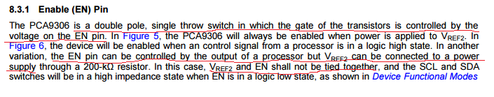
I see some conflicting information in the datasheet of the PCA9306.  On page 8 of the PCA9306 datasheet it states:

"the EN pin can be controlled by the output of a processor but VREF2 can be connected to a power
supply through a 200-kΩ resistor. In this case, VREF2 and EN shall not be tied together, and the SCL and SDA
switches will be in a high impedance state when EN is in a logic low state"

But, then I see it also states on page 11 the following:

"For the bidirectional clamping configuration (higher voltage to lower voltage or lower voltage to higher voltage),
the EN input must be connected to VREF2 and both pins pulled to high-side VDPU through a pull-up resistor
(typically 200 kΩ)."

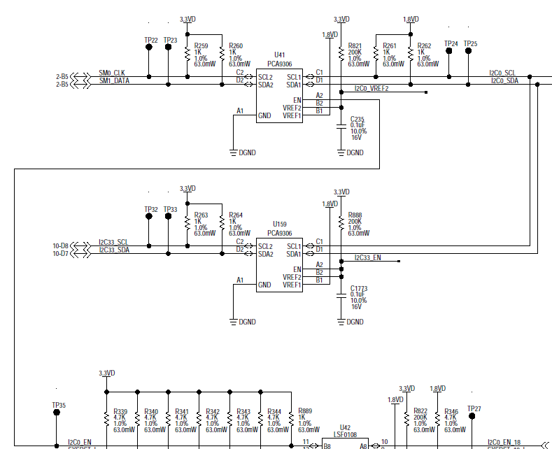
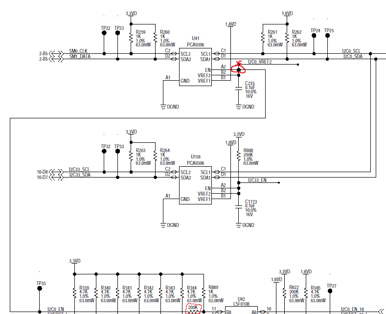
In my design below I hooked it up as it states I can above from the datasheet from page 8.  The value of the EN input is 3.3V, however, the value at R821 is 1.8V.  That means that the VDPU is NOT VREF1+0.6V as VREF1 and VDPU are now both 1.8V.  

Could I drive the EN and VREF2 from the output of the LSF0108 directly? 

Thoughts?

  • Hello Matt,

    Thanks for making the new thread.

    1) On page 8, I think you may have over looked the sentence that states you can use it as a DTST switch by disconnecting EN and VREF2. I agree that the wording is confusing/not clear and I am going to be updating this datasheet to fix bad wording like this. 

    The correct verbage should say something like: If you wish to use the PCA9306 as a double pole single throw switch with no voltage translation, then EN and VREF2 may be disconnected and a control signal from a processor can be used to control the switches. The switch will go to high impedance with EN signal low.

    2) In your second paragraph: "For the bidirectional clamping configuration (higher voltage to lower voltage or lower voltage to higher voltage),
    the EN input must be connected to VREF2 and both pins pulled to high-side VDPU through a pull-up resistor
    (typically 200 kΩ)."

    This gets the point across a little better, and highlights that to perform voltage translation, the EN and VREF2 pins must be connected together.

    3) You are seeing 1.8V at the VREF2 pin because your EN pin voltage is too high to perform translation. With the EN and VREF2 pins connected together, the device self regulates itself to bias the EN pin to ~VREF1 + 0.7V. If they are disconnected and you apply a voltage higher than VREF1 + 0.7V to the EN pin, then you will fully turn on the translation gate, causing it to go to low impedance, which will make the VREF2 pin have a voltage of VREF1 with the 200k series resistor to the VDPU.

    4) Technically, you should be able to drive EN and VREF2 from the LSF device (they pull very little current). If you need translation across the device, it is important that EN pin be biased to approximately VREF1 + 0.7V (whether applied with external components or via the VREF2 pin.

    To fix your translation issue, you will have to get the EN pin voltage to the appropriate value (~2.5V), which I see the following options:

    • Correct schematics to  EN/VREF2 shorted, and then pulled up to 3.3V through 200k ohm resistor.
    • Cut EN trace and short EN to VREF2 pin.
    • Resistor divider somewhere on board to provide voltage to EN pin.

    You did U159 correctly, but one important note is that the I2C33_EN line must not drive the node high. It must be an open-drain and only pull the node to ground or release it to let the device self-regulate.

    One last note: Your pull-up resistors are very high in value (1k), and when a slave broadcasts a 0, it will have to sink the current of both sides of the PCA device. Since you have multiple PCA devices, this current will be very high: (3.3/ 1k + 1.8/1k + 3.3/1k) = ~8.4mA. I would highly advise raising these pull up values to at least4.7k ohms or you may have issues with slaves that have higher RON pull-downs.

  • So, for the LSF0108 to drive the EN/VREF2 all I would do is remove the 1k ohm resistor and use the 200k ohm resistor to pull up EN/VREF2 to 3.3V?
  • Actually, the LSF0108 is an open drain device very similar to the PCA9306. You will need to keep the 1k pull-up in order to power the line, a total impedance of 201k to 3.3V won't make a difference. If you can short EN/VREF2 and then pull it up to 3.3V from the LSF0108 output (tied up to 3.3V through a 1k pullup).

    I would also either verify that I2C0_VREF2 line does not draw any current or I would disconnect it from the node.

  • I2c0_vref2 is just a net name and not connected elsewhere. Your schematic edit is confusing me as you say to keep the 1k resistor, but then marked it out with 200k. Please be explicit in your recommendation reply.

    Thank you!
  • Whoops.

    I did write the wrong thing, sorry. The choice you take will depend on how you control the LSF0108. Does the A side of the node that controls the enable stay high? Do you only enable the switches when you want to pull the line low?

    My concern with the method I put in the diagram is that if you leave the EN high on it. Then the voltage at the B8 node will be VREF1 + 0.7 which will likely be enough to activate the gate of the LSF0108 and then we will have the same problem we have now.

    If you can put a 200k series resistor and leave the 1k pullup to 3.3V, I believe this would be safe in all cases, then when you send a 0 on the A8 side, it should pull the B8 node low to disable the PCA9306. See updated schematic.