Because of the Thanksgiving holiday in the U.S., TI E2E™ design support forum responses may be delayed from November 25 through December 2. Thank you for your patience.

This thread has been locked.

If you have a related question, please click the "Ask a related question" button in the top right corner. The newly created question will be automatically linked to this question.

Correct way to wiring PCF8575 as input

Other Parts Discussed in Thread: PCF8575, TCA9555

Hi everyone,

Reading the datasheet of PCF8575, it is not clear the way to connect PCF8575 as input ports. In the datasheet, a push-button and pull-up resistor is connected between 2 VCC. Also, I didnt found any others suggesting to do that.

May I connect the input port only with a pull-up resistor ou pull-down resistor ? Or it should be connected in a voltage divider ?

Thanks.

  • Hello Daniel,

    Thanks for the question.

    The reason why you saw a push-button and a pull-up resistor is because a CMOS input must be at a known voltage at all times. If the node is left floating, it can cause excessive current draw and an unknown input state.

    For this reason, it is very common to have a pull-up resistor (typically high value: 10k to 100k) on an input line connected to a push button. The push button then connects to ground when pressed, which will force the node to either be at VCC when button is released, or at ground when button is pressed.

    You do not want to use a voltage divider network as ideally, the input voltage applied to a CMOS input should be either at GND or VCC voltage. You typically will use a pull-up resistor and a button that connects to ground when pushed, as this is considered 'safer'.

    It's safer because the current flowing through the switch will be low, even if the node accidentally gets shorted to ground.

    Consider a switch that connects to VCC and the node has a pull down resistor, if the switch were to get internally shorted to ground (as the chassis pins on the switch are normally soldered to the ground plane), then you can get a significant amount of current flowing through the switch.
  • Hello Jonathan,

    Thanks for your replay.

    Ok, I will prototype with pull-up configuration.

    Thanks again.

    Daniel Thomazini

  • Hello Jonathan,

    As you suggested, I tested the PCF8575 inputs with pull-up resistors. As expected, the value went from 1, with push-button open, to 0 when the push button was closed. 

    As the pin were put high to input configuration, as requested by the datasheet, the pull-up resistors are not effective, because this configuration is imposing the same signal to the pin. So, I removed the resistor, and the pin was connected to push-button -> GND, and this configuration also worked as the same before. I'm afraid due to the current in both cases, so, is it a problem ?

    Thanks again.

    Daniel Thomazini

  • Hello Daniel,

    Could you explain this again, I don't quite understand.

    You tested the PCF with pull-up resistors, and value was as we expected. Can you explain if you had the ports setup as inputs or outputs?

    "as the pin was put high to input configuration, as requested by the datasheet". If you have the port setup as an input, the PCF device should not be pulling the line high. If you removed the resistor, and the line still gets pulled high after you press the button, this likely means that the device has the output driver set high, and when you press the button, you short the driver to ground, causing the input to read 0. However, you are sinking a very large amount of current when you do this! In this case, you will damage the device.
  • Hello Jonathan,

    Before the test, the pins of the PCF8575 were put in HIGH, writing 0xFFFF to the PCF.

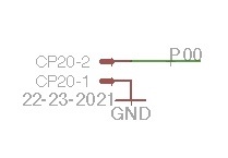
    As you suggested, I did the follow setup:

    where CP20 is a push-button. This configuration worked as you said, when reading the ports the values were 1, and when the push-button was pressed, this bit goes to 0.

    As P00 is HIGH, or 5VDC, I removed the resistor:

    and the result was the same. The current that flows from pin to GND could be a problem ?

    Thanks again.

  • Hello again Jonathan,

    I was reading the datasheet more carefully, and it is obvious, you are absolutely right. For input, the pins must be pulled-up to avoid high current.

    Thanks again.
  • Hello Daniel,

    Another thing I would like to bring to your attention (this slipped my mind, my apologies) is that this device does not have registers to allow you to control/disable the output drivers (current source). This part is not ideal for being used for many buttons because of this. Each button you press will have ~100mA of current flowing to ground. Bottom line: this setup you have should be ok, but not ideal.

    If you are wanting to use an IO expander purely for reading button presses, I would highly recommend taking a look at another one of our IO expanders that have built-in pull-up resistors, which can help cut down on current consumption, if that is a concern for you. I would look at the TCA9555, as it is very similar to the PCF part, but some software changes would be necessary, because the TCA device uses internal registers in order to configure the part. This gives you more control over the ports, unlike the PCF's approach.
  • Hello Jonathan,

    Thats perfect !!!  I think that TCA9555 is the vital component to my project, because I will use all pins as input with push-buttons.

    I was reading  the datasheet and I have a doubt: the internal pull-up resistor are already active by default, or it is necessary to active them by the registers ? In the " SIMPLIFIED SCHEMATIC OF P-PORT I/Os" picture, I think that it is always active, and the Q1 and Q2 will be off to input configuration. So, I can only connect the pin -> push button -> GND ?

    Thanks again.

    Daniel Thomazini

  • Hello Jonathan,

    I was wondering about how to use all PCF8575 pins as input with push-buttons. Looking at the figure 8.2.2, the main problem, as we already discussed, is the current between VCC and GND.
    So, I use a 10k resistor between voltage source and VCC of PCF, to reduce the total supply current to the PCF. The total amount of current measured was 0,37mA when all pins were directly connected to the GND.
    Do you believe that this configuration will damage the PCF8575 ?

    Thanks again.

    Daniel Thomazini
  • Daniel,

    The pull-up resisotrs in the TCA9555 are always active. If you wish to have the ability to independently configure which ones are active or not, there are some other IO expanders we can look at, which support this.

    In regards to measuring your current, What I think you need to measure is not just the current flowing from VCC to ground through the resistor, but you should also measure the current to ground through the switch (including the current that flows out of the IO port on the PCF device). The PCF device will source some current as well, and my concern is actually the internal current source on the PCF device will have a large amount of current.

    0.37mA is in line with what we would expect from a 3.3V rail with a 10k pull-up (330 uA of current). This pull-up resistor current is very small, it is the current coming out of the PCF IO pin that had me concerned.