


Other Parts Discussed in Thread: ISO1540
Hi,
We had some difficulty on how iso1540 works. On the datasheet diagram the right has a delay where SDA1 stays ≤VOL1 , and it can only rise above VOL1 after SDA2 rises above ITH2, and there is a red dotted “receive delay” marking the short delay time in diagram.
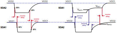
First, is the “flatter” area where SDA1 stays ≤VOL1 basically due to: there is a voltage contention between the driving source of SDA1 and the open drain output of transistor B. Before the rise of SD1, when SDA1 stayed low, the drain of the MOSFET on the left of B is at 0.75V, this requires that the output of A MUST >0.75V+Vgsth to be turn on the MOSFET. This is the main factor contributing to the “flatter” delay. Please confirm this.
And for how the design avoids self-latch, I can see when left side (SDA1/SCL1) cannot be latched at LOW output because floating voltage, if we assume a 0.75V, does not qualify LOW for C comparator, so this invalidates any self-latching. Basically the offset breaks the symmetry. Conversely SDA2/SDA2 cannot be latched LOW either.
But HIGH seems can be self-latched, bidirectionally? Please confirm on both HIGH/LOW latch.

