This thread has been locked.

If you have a related question, please click the "Ask a related question" button in the top right corner. The newly created question will be automatically linked to this question.

TCA9517 Input/Output Capacitance for the EN Status

Other Parts Discussed in Thread: TCA9517

Hi,

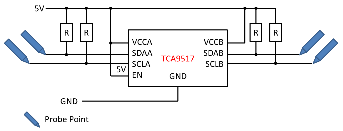
Could you please tell us why the input / output capacitance for SCLA and SCLB is 3nF ~ 15nF depending on the enable status since this result was different with the value which is mentioned in the data sheet when our customer has evaluated those capacitance for their pins as below ?

(1) Initilal Condition
- VCCA/VCCB = 5V
- Unmounted Pull-up Register for SCL*/SDA*

(2) Results
- Case of EN = 0V
   SCLA = ~11pF
   SCLB = ~11pF

- Case of EN=3.3V
   SCLA = ~3nF
   SCLB = ~15nF

Best regards,
Kato

  • Katosan,
    Very interesting that they find large difference in capacitance.

    Could you explain their capacitance test setup and what device they are using to test? Things like frequency, DC bias, voltage applied to other pins, are they using a VNA or a RLC'? They should not get any capacitance measurements in the ~35 nF range at all, which leads me to believe something is being measured differently from us.
  • Hi Jonathan-san,

    Thank you for your quick response.
    I will confirm whether our customer has evaluated the capacitance at 1 MHz with a 1Vrms signal and will get back to you.
    However, I believe that TCA9517 has any causes since our customer has evaluated it in the same conditions.

    Best regards,
    Kato

  • Hi Jonathan-san,
    I will update our customer information.
    The overview of evaluation schematic is shown as below.
    He has evaluated the maximum capacitance of DDC(SDA*/SDL*) according to the HDMI compliance test specification version 1.4 .
    As a result, one for A-side port is ~50pF, other for B-side is ~nF order.
    Should not TCA9517 be adapted for the HDMI applications ?
    Could you please give me your advice ?
    Best regards,
    Kato
  • Hello Kato-san,

    Their measurements still do not seem correct. I know that capacitance of the device at the B port is 8 to 13 pF. If they're getting a nF measurement, something is wrong with either
    a) the measurement setup
    b) the layout of the device (not that a low resistor to a large power supply cap load can increase capacitance). Make sure there are no stubs in the layout.
    c) the device itself.

    I would suggest checking the capacitance without the pull-up resistors on the B side to check and see if that affects the reading.

    The A side and B side are designed to have identical pin capacitance.
  • Hi Jonathan-san,

    Thank you for your support.
    We will discuss this issue with our TI local office member and will contact you again.

    Best regards,
    Kato