This thread has been locked.

If you have a related question, please click the "Ask a related question" button in the top right corner. The newly created question will be automatically linked to this question.

SN65DSI84 LVDS waveform generation-related

Other Parts Discussed in Thread: SN65DSI84, SN65DSI83, SN65DSI85

Hello!

For us, please contact the LVDS waveform issue

< check way >

1) When passing the MIPI Video Signal in Black pattern. 

2) The initials Write of the SN65DSI84 IC 

< result >

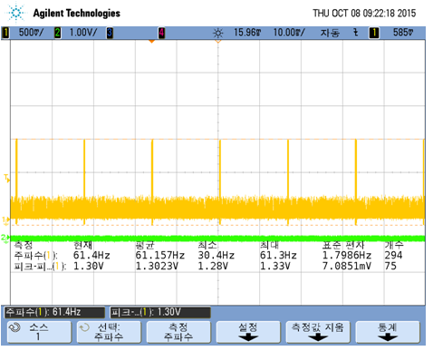
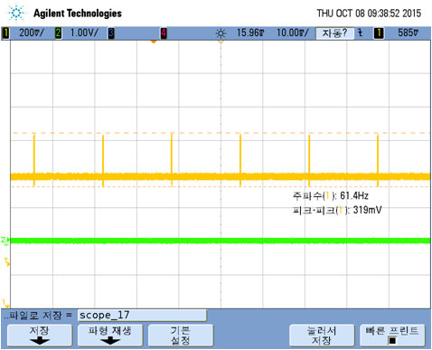
LVDS waveform of A_Y0P / N line of problems that Data is output per 60Hz.

< Reference materials >

1)  MIPI - Black Pattern

2) LVDS - A_Y0_P  line

please answer about my question.

  • Can you provide an capture of DSI CLK input?

    Regards,

  • Thank you.

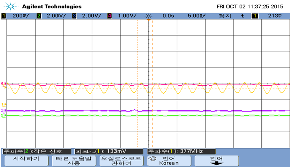
    The current DSI CLK is 377MHz.

    See the picture.

    Please tell us if you need more details.

  • Could you check if SN65DSI83 test pattern is OK?

    FYI, init sequence as below:
    1. After power is applied and stable, all DSI input lanes including DSI CLK(DA x P/N, DBx P/N) must be drive to LP11 state.
    2. Assert the EN pin.
    3. Wait for 1ms for the internal voltage regulator to stabilize.
    4. Initialize all CSR registers to their appropriate values based on the implementation.
    5. Start DSI video stream.(init seq5).
    6. Set PLL_EN = 1
    7. Wait 3ms for PLL to lock.
    8. Set the SOFT_RESET bit

    A few things you can try:
    - If DSI input is being affected by the EMI/noise, try to adjust the EQ value at addr 0x11. Default is 0x00 with no equalization, try 01b or 11b and see if the issue improves on both DSI_DATA and DSI_CLK
    - If there's noise issue on LVDS output/panel input, the LVDS_VOD swing can also be adjusted at addr 0x19.
    - It is important that all DSI signals are in LP11 state prior/during EN assertion/de-assertion. Even if all registers are set up correctly and PLL is locked, video will not get passed through from DSI to LVDS if this requirement is not met.

    Is PLL_UNLOCK bit set?
    Can you provide a register dump when the intialization sequence is completed?
    Is EN= high stable? Is VIO18_PMU stable?

    Regards,
    Joel
  • Thank you for answer.

    < DSI Information >

    MIPI 8Lane

    1440*2560

    MIPI CLK : 389MHz

    MIPI LP CLK : 10MHz

    VBP : 46

    VFP : 10

    VSW : 2

    HBP : 56

    HFP : 104

    HSW : 20

    < Initial setting current >

    1) POWER ON -> DA x P / N, DB x P / N LP11

    2) En Pin ( High)

    3) Delay(25)

    4) Initial setting current  

    REGS.WRITE(2, 0x09, 0x00)

    REGS.WRITE(2, 0x0D, 0x00)

    REGS.WRITE(2, 0x0B, 0x48) //35MHz

    REGS.WRITE(2, 0x0A, 0x03)

    REGS.WRITE(2, 0x10, 0x26)
    REGS.WRITE(2, 0x11, 0x44)
    REGS.WRITE(2, 0x12, 0x4F) // 110.5MHz(0x16)
    TIME.DELAY(2)
    REGS.WRITE(2, 0x18, 0x6c)
    REGS.WRITE(2, 0x19, 0x05)
    REGS.WRITE(2, 0x1A, 0x03)
    REGS.WRITE(2, 0x1B, 0x00)
    TIME.DELAY(2)

    REGS.WRITE(2, 0x20, 0xD0) 
    REGS.WRITE(2, 0x21, 0x02)
    TIME.DELAY(2)
    REGS.WRITE(2, 0x24, 0x00) 
    REGS.WRITE(2, 0x25, 0x0a)
    TIME.DELAY(2)
    REGS.WRITE(2, 0x28, 0x20) 
    REGS.WRITE(2, 0x29, 0x00) 
    TIME.DELAY(2)
    REGS.WRITE(2, 0x2C, 0x14) 
    REGS.WRITE(2, 0x2D, 0x00) 
    TIME.DELAY(2)
    REGS.WRITE(2, 0x30, 0x02) 
    REGS.WRITE(2, 0x31, 0x00) 
    TIME.DELAY(2)
    REGS.WRITE(2, 0x34, 0x38) // HBP
    TIME.DELAY(2)
    REGS.WRITE(2, 0x36, 0x00) // VBP
    TIME.DELAY(2)
    REGS.WRITE(2, 0x38, 0x00) // HFP
    TIME.DELAY(2)
    REGS.WRITE(2, 0x3A, 0x00) // VFP
    TIME.DELAY(2)
    REGS.WRITE(2, 0x3C, 0x00)

    5) MIPI Video Signal Start

    6) ~ 8)

    REGS.WRITE(2, 0x0D, 0x01

    TIME.DELAY(5)
    REGS.WRITE(2, 0x0A, 0x83)

    REGS.WRITE(2, 0x09, 0x01)

    It fits that setting as shown above?

    Due to the dual-mode half reduced resolution settings. 

  • Please, provide your panel 's datasheet.

    Regards,
    Joel
  • Thank you for answer.

    Setting tried to re-model change.

    Please check the current settings are correct.

    Note to attach to the material DataSheet.

    Model Name : LMS480JC01

    < DSI Information >

    MIPI LANE : 4Lane

    LCD Size : 1024 * 600

    VBP : 4

    VFP : 3

    VSW : 1

    HBP : 80

    HFP : 48

    HSW : 32

    MIPI HS CLK : 66MHz (132Mbps)

    MIPI LP CLK : 10MHz

    MIPI Pixel CLK : 44MHz

    < SN65DSI85 Setting >

    0x09            0x00
    0x0A            0x05
    0x0B            0x00
    0x0D            0x00
    0x10            0x20
    0x11            0x00
    0x12            0x0B
    0x13            0x00
    0x18            0x70
    0x19            0x00
    0x1A            0x03
    0x1B            0x00
    0x20            0x00
    0x21            0x04
    0x22            0x00
    0x23            0x00
    0x24            0x00
    0x25            0x00
    0x26            0x00
    0x27            0x00
    0x28            0x20
    0x29            0x00
    0x2A            0x00
    0x2B            0x00
    0x2C            0x20
    0x2D            0x00
    0x2E            0x00
    0x2F            0x00
    0x30            0x01
    0x31            0x00
    0x32            0x00
    0x33            0x00
    0x34            0x50
    0x35            0x00
    0x36            0x00
    0x37            0x00
    0x38            0x00
    0x39            0x00
    0x3A            0x00
    0x3B            0x00
    0x3C            0x00
    0x3D            0x00
    0x3E            0x00

    0x09            0x01

    0x0D            0x01

    The currently displayed image.

    LMS480JC01.pdf