This thread has been locked.

If you have a related question, please click the "Ask a related question" button in the top right corner. The newly created question will be automatically linked to this question.

TUSB1210 - VDD15 beyond limits and DIR does not come LOW..

Other Parts Discussed in Thread: TUSB1210

Hi all,

In my power up sequence of TUSB1210, DIR does not come low at times and VDD15 gives = 1.9V why??? Chip is not heating at all...

My power up sequence is as follows, I am detailing power up sequence only cause here is where I guess there may be some issue:-

1) I keep resetb low and STP ='1'. My CS is always tied to 1.8V.

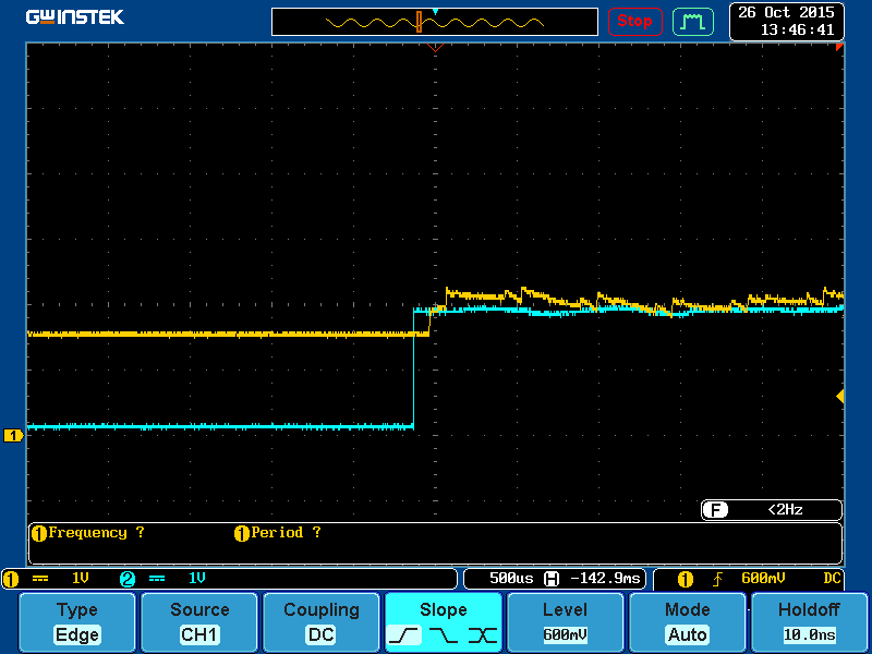
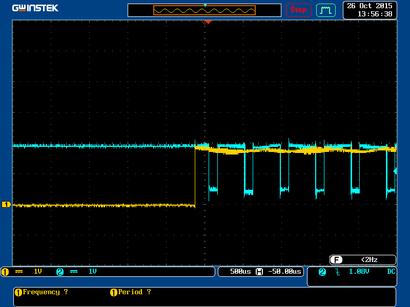
2) When I check for DIR high, I wait for 3ms  and then RESETB  = '1' along with CLK = 60MHz.. Here many times I find that VDD15 = 1.9V [PROBLEM]. DIR Some times even stucks at one and does not come low at all even though STP remains high

CAP at VDD15 = 4.7uF ceramic ..

Why VDD15 goes beyond limit and why DIR does not come low - PLL Does not lock or what??

I have checked other voltages - fine - 3.3V and 1.8VDC. My VDD33 and VBAT sre shorted externally. I have even changed the chip twice, same results. i use EVM from TI for TUSB1210 and club it with FPGA..

I switch on 3.3V and then 1.8V through two separate switches one after the other.

I will start a separate thread for this as well, you may reply there..

Regards.

  • 1) Can you confirm the FPGA IO voltage really is 1.8V and that the relevant IO power supplies on your FPGA is 1.8V?

    2) For info, after DIR goes low after reset, I wait for a RXCMD before writing to any registers. Can you delay each register write so you can associate the out of range Vdd15 with each register write operation?

    3) How long after de-asserting reset does DIR go low?  The datasheet suggests a nominal 0.54ms.

  • Dear Mike,

    1) I can confirm the IO Volate to be 1.8V and there are level translators that translate between the FPGA and TUSB1210 from 3.3V to 1.8V which are 100MHz capacity.

    2) To show the scenario I attach two oscilloscope waveforms:-

    1) First one shows resetb (blue) with VDD1.5 (yellow). VDD1.5 is initially stable at 1.5V before resetb is made high. As resetb goes high, many times it jumps to 2.0V [as here] and sometimes it remains at 1.61V.

    2) Second one shows resetb (yellow) with DIR (blue). As reset goes high DIR come low and starts toggling even if i do not write anything on TXCMD. This toggling happens when VDD15 goes 2.0 V. Else it toggles once and then DIR remains high permanently.

    Mike can you tell me :- I use Clock Input Mode so whether the clock should be exactly 60M +/- 15K or whether it can be +/- 30K.

    Hope to egt some insight from you.

    Regards

  • DIR Comes low much before 0.534ms. Say around 250uS. What can this imply?

    Regards
  • Why are you using interface ICs between the TUSB1210 and your FPGA? You can get PHYs with alternative IO voltages. The FPGA I used could cope with 1.8V, which one are you using?

    I'm surprised at the fast rising edges of VDD15. I would have thought your 4.7uF cap would slow them up somewhat. Can you confirm you have used a ceramic capacitor?

    I also use clock input mode. I use a FPGA DCM to create the 60MHz clock. Something I'm aware its not ideal, but in theory the jitter should be small and should be within datasheet tollerances. It is possible that this causes issues as the PHY will have a buffer to cope with differing speeds between clock and data rate and I don't know the internal architecture of how it copes.

    Have you looked at the clock on a 'scope? Is it clean? The datasheet does say 250ppm for Input Clock Configuration so I assume +/-15kHz.

    What you are saying, is that despite holding all signals low during apart from applying clock, after reset VDD15 is noisy 100us or so after nReset goes high?

    I'm left wondering how well the power supplies are decoupled and how well the pad underneath the device is connected to ground?

    Anything more and I'm stumped.
  • Dear Mike,

    I am using saturn spartan 6 from numato where no FPGA banks have I/O of 1.8V and so had to level Txs.

    Yes I am using X7R dielectric based 4.7u ceramic. The funny part is when I see a DIR low - high - low and then if i write a command say as you said - 40H to 84H, I find DIR stops at a H, does not toggle any further and VDD15 is also steady at 1.62V.

    Clock seems to be clean but when seen on scope it shows a variation of +/-30KHz.. I am also using DCM. Saturn Spartan 6 uses crystal 100MHz with 25ppm stability which i think is good. Is there some way in usage of DCM, accuracy can be improved by using some combinations of M and D or some other way.

    PAD is well connected, no issues there, I can improve decoupling further as you said.

    Mike, can you give me your email ID in case I want to share my VHDL development with you regarding this for some inputs as to how you are maintaining the clock phase of the internal data generated by S/M going out and the clock signal input to PHY - whether they are in the same phase or 180 phase apart and other issues as well..

    Regards.

  • Hi Mike,

    I have done two things:-

    A) Further introduced Filtrers for decoupling.

    B) Removed resistances on data and control lines 22 ohm as given by texas EVM.

    This has brought stability in the results [I do not see sporadic things happening] and I am able to see the value of DATA RXCMD during DIR Toggle, earlier most of the times it remained to 00H. Although the problem raised in this post is still there unless I DO NOT WRITE A TXCMD TO FUNCTION CONTROL REGISTER. However, if i write one DIR gets locked to '1'.

    BUT I WANT TO SHOW ONE THING

    Please see the below snapshot of chipscope, once I give the resetb = '1', DIR goes low [NOT SHOWN] and then toggles as marked in the blue ring. Then I see RXCMD - 24. When I am using my PHY as a peripheral, why HOSTDISCONNECT interrupt must come? I have disconnected ID pin, CPEN pin. Is it not enough to configure PHY as peripheral???

  • Just sent you a message through this site. Hope you get it.

    Why is there a mis-match between DIR and the data? I would expect DIR to be high for 2 clocks, and the data to be valid for the second clock period, not after DIR going low. Is this because of your buffers? I'm concerned that other timing, like NXT might be awry causing your TXCMD issues. How confident are you the clock - data relationship is correct?

    Are the buffer direction pins driven directly by DIR?

    The simple fact you have improved decoupling and seen an improvement is key. Are you using a 4 layer board? How close is your decoupling to the IC?
  • Yes I have received the message. Thanks.

    All the signals are as on the pins EXCEPT DATA. DATA is clocked and then shown hence you are seeing a delay between DIR/NXT/STP and DATA. So thats ok according to me.

    These level translators are auto direction level translators - MAX3013, 100Mbps so I have no control over direction.

    Texas EVM had not placed it very close to the IC, so i could not.. I will send you the PIC of my board on your ID.

    I have increased the decoupling upto 47uF at all points.

    Regards.
  • The board is 4 layered...
  • The MAX3013 seems quite a high speed device, but also has quite a low input impedance on the the LV side. The TUSB1210 data bus has a limited drive capability. I have never used this sort of device before and wouldn't normally consider the complication, or the cost given the alternative PHYs on the market that have more sensible IO voltages.

    Just increasing the capacitance doesn't necessarily help. ESR is probably more important, hence essential to use ceramic caps.

    I don't feel I have much more to add!

  • Dear Mike,

    There is certainly more that you can highlight on:-

    I have found that the commands that I write are not reflected in the registers when I read. Just Check the below chipscope image. After DIR toggles and goes low for the first time after resetb = '1' raised, I first check for OTG register value and I read 06H. Then I write a clear command to it and then again I read it. I still get 02H. Data bus is delayed by one clock cycle in the timeline. The reason I checked for OTG is that whenever, DIR starts toggling after power on reset and and VDD15 goes to 2.0V, I find Host Disconnect interrupt from the PHY. I am not clear still as to what is the cause and which is the effect.

    Regards.

  • However, with your suggestion, I have ordered a few USB3320 so that I can remove the level translator hassle.

    Regards.
  • I hear what you say about the data being a clock late, but it bothers me to see "8C" for what looks like 3 clocks rather than 2.


    Also the NXT high for one clock before a DIR?

  • Dear Mike,

    I would first like to thank you for the amount of effort you took to understand the problem. The problem was the grounding of the underneath pad and better decoupling which has sorted out my problem 4 days back but I got time today to reply.

    Thanks for all the effort and giving me right guidance so that I could remove noise from my brains regarding clock accuracy and concentrated on basics, asked technician to correct it, problem solved...

    Regards to bhaumik darji as well..

    Regards.
  • Hi,

    Pleasure. The TUSB1210 is quite a mature device and the TI team or design house that designed this IC have long gone or disbanded. Shame they don't retain any expertise but I guess that's a sign of the times.

    I recall mentioning about connection to the pad as I recall that is the only Ground connection the IC has.

    I'm pleased you seem to have sorted things out.

    Regards

    Mike