This thread has been locked.

If you have a related question, please click the "Ask a related question" button in the top right corner. The newly created question will be automatically linked to this question.

DS90CF383B TxCLKIN vs TxCLKOUT+/-

Other Parts Discussed in Thread: DS90CF383B, DS90CF386, DS90CR218A, DS92LV2411

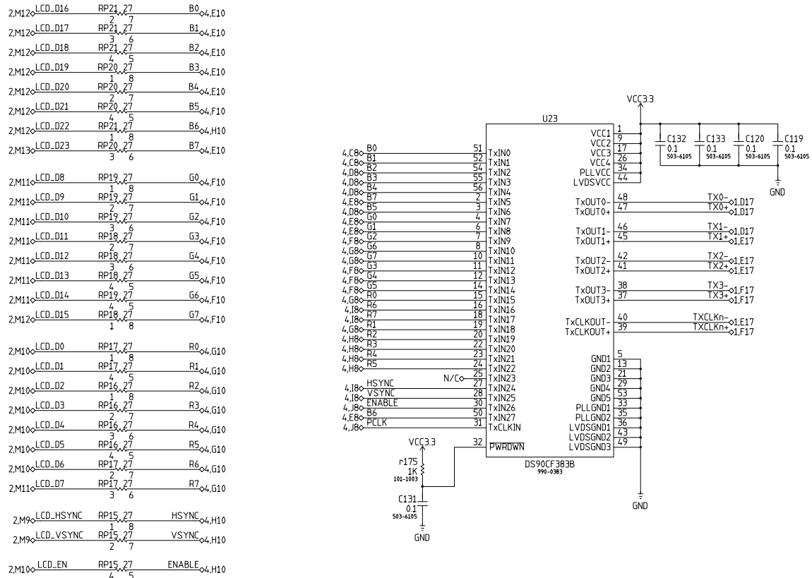
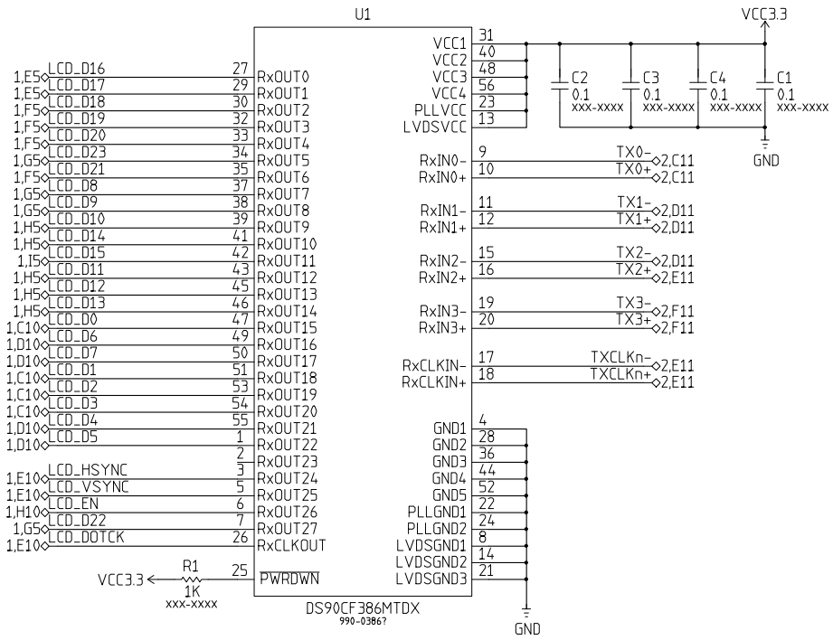
I have a product that was driving a display directly through an RGB type connection, the system architecture has changed requiring the use of LVDS across a cable (12" long) to the display. I am using a DS90CF383B LVDS Transmitter connected to a DS90CF386MTDX Receiver which I am attempting to run with a TxCLKIN at 19Mhz.  What I see on the display is unrecognizable "moving fuzz".   

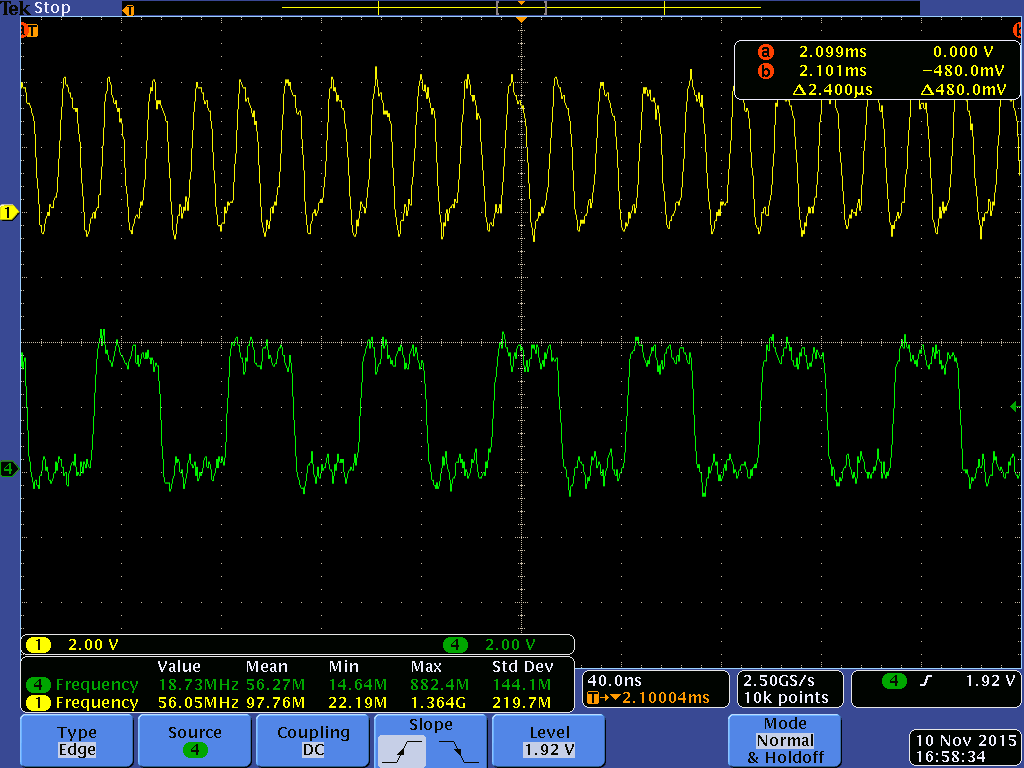
To troubleshoot this I've confirmed that the cable pin out is correct between the two controllers.  I noticed that while I'm inputting a Dot Clock (TxCLKIN) of 19MHz, I'm getting out a Dot Clock of 56MHz out of the receiver....  Additionally the TXCLK+/- signal appears to be running at 19MHz.  I believe this differential clock should be an order of magnitude 7 times higher then my TxCLKIN to transmit all 24 bits of color data.  It looks like the internal PLL is not locking for some reason. 

Could someone provide me some with some assistance to help guide my debugging?

Thanks,

Mark

TX Schematic

RX Schematic

  • Here is the scope trace of the RX dot clock (yellow) and the TX dot clock (green)

  • Hi Mark,

    I believe your problem could be coming from two different sources.

    First, the DS90CF386 LVDS receiver supports a 20 MHz – 85 MHz shift clock. Your clock is outside of this range at 19 MHz.

    Second, each LVDS input and output must have a 100 Ω termination. This resistor terminates the differential lines with their characteristic impedance. This termination resistor is necessary in order to probe and measure LVDS signaling. Without the 100 Ω differential termination, you are creating an open circuit, and the signals could be distorted.

    Thanks,
    Katelyn
  • Hi Mark,

    As an addition to Katelyn's response, the LVDS clock output from TXCLKOUT should be at the same frequency of TXCLKIN. When the LVDS clock is received by the LVDS deserializer chip, the internal PLL onthe Rx will scale up the clock x 7 and sample the incoming LVDS data signals according to the Rx strobe positions for each bit in the LVDS clock cycle. If the incoming clock is out of the LVDS receiver lock range, as Katelyn mentioned, the receiver may not be able to lock.

    Thanks,

    Michael
  • Michael/Katelyn,

    Thank you for your responses!  I've added 100 ohm terminations and am now seeing the same dotclock output from the RX chip as is being input to the TX chip.  We have also bumped the clock up to 26MHz for testing purposes as well.   The display looks closer to what I would expect but its still not quite right, I am in the process of comparing all of the data lines on the TX and RX side to find out which is the culprit.

    Out of curiosity, is there a 56pin TSSOP device you would recommend as a drop in for the part(s) I am currently using which would allow me to run at lower than 18MHz (10-15MHz) ?

    Thanks

    Mark

  • Hi Mark,

    Unfortunately, there does not appear to be a part that meets the exact description of being a drop-in replacement with a 56-pin TSSOP.

    The only options for receivers that operate down to 18 MHz or less I notice in the portfolio are the DS90CR218A (TSSOP, but only 3D + C LVDS pairs) and DS90C3202 (uses TQFP and has 9 LVDS pairs).

    If you are still open to design suggestions, may I suggest another Tx/Rx approach? You will be able to achieve this 18 MHz operating frequency in an easier way by upgrading to a Channel Link II Tx/Rx pair, where all the serialized data and clock are encoded onto 1 high-speed CML pair. Not only will you be able to run at your desired 18 MHz frequency, but you also will not be burdened with the meticulous care required to mitigate as much pair-to-pair skew as possible in the Channel LInk I/FPD-Link I devices. For example, please give the DS92LV2411/12 a look.

    Thanks,

    Michael

  • Thanks Michael,

    The display is successfully working now. The terminations helped, timing of the signals has slightly changed from driving RGB to putting the LVDS in between now. When we invert the data enable signal to the display, everything worked great.

    I am going to be redesigning the product as I also had to lower the display dotclock to 7MHz. To get this to work with the LVDS controller I re-routed the signal in as if it was a data signal, then provided a separate 100MHz clock to the LVDS chip. I am now looking at spinning the PCB to incorporate your DS92LV2411/12 suggestion. It appears that I can drive this with the 7MHz dot clock .

    Thanks to everyone for all the help!
    Mark