This thread has been locked.

If you have a related question, please click the "Ask a related question" button in the top right corner. The newly created question will be automatically linked to this question.

DisplayPort Buffer recommendation

Other Parts Discussed in Thread: SN75DP118, SN75DP120

Hello,

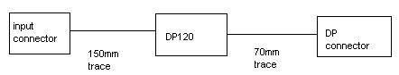
I have a need for both a RX and a TX DisplayPort buffer.   I am considering both the SN75DP118 and the SN75DP120.  The DisplayPort endpoint will be about 8 inches from the connector, where i intent to put the buffer.

I dont see how teh SN75DP120 is useful for any DP transmitter because the endpoint itself is required to do the pre-emphasis and amplitude adjustments.  the only reason that i could see to use this part is if you want to bolt it to some device that is only partially DP compliant.  I get the feeling that i must be wrong here.  Could someone correct me please.

The SN75DP118 is interesting as long as it is a wave form follower.  In other words, it should replicate the pre-emphasis and amplitute that is sees on its inputs.  Is this the case?  The only thing that i worry about here is that the signal from the DP endpoint will overdrive the DP118 because its amplitude and pre-emphasis are set to drive a cable.  Can the buffer handle signals like this?

Anyway, I woudl appreciate any advice you could give for my application.

Thanks!

Aaron

  • Aaron,


    So depending on what you want to do and what you have to work with, the DP118 or the 120 could be you solution.


    The DP118 is a true voltage follower with the ability to follow all of the amplitude and pre-emphasis of the DP signal.  It will provide minimal ISI correction.

    The DP120 is a true redriver (does not have a CDR so it is not a re-timer).  The DP120 was design to monitor (sniff/listen) the AUX communication and mimic the DP transmitter settings.  In general this is the device used for re-driving a signal as it has a full driver circuit with full amplitude and emphasis settings controlled by the AUX communication.  Both of these devices usually sit inside a laptop next to the external DP source connector and recondition the signal as it is sent out to the receiver.  The DP120 is a full reconditioning device, while the DP118 is a voltage follower with minimal correction of the signal.


    We have an EVM if you would like to look/test the behavior to decide the most appropriate for your design.


    Ken

  • Ken,

    Thank you for your response.  It sounds like the DP120 is the part to use at the transmitter and potentially at the reciever.  First of all it is powered with 3.3V, so that is much easier to get a clean power in a system that uses 12V, 5V, etc...

    The easy question is this - can the part be used without hooking up the aux bus so that the amplitude and preemphasis stay at the default setting, but the RX EQ is used?

    The harder question is this - how does the device act when glued to a DP compliant device that does not know that the DP120 is there?  If the DP tranmitter is adjusting its amplitude and pre-emphasis, it seems like it would overdrive teh DP120.  Can you please explain how this works?

    Perhaps a quick conference call would work best.

    Thanks!

    Aaron


  • Aaron,


    We can have a conf call if  you like, just let me know.


    DP120 will have absolutely no issue with connecting up to a compliant DP source (amplitude and or pre-emphasis), as this is the way it was designed (you can also have a fixed input, but this is not normally implemented to date... requires a software instruction different from the normal compliance mode).  It was not necessarily designed to be part of a receiver at the other end of a cable.  I have heard of customers using the DP120 in that fashion, but I haven't had any feedback as to how successful it was.  The source side interface of the DP120 has some equalization built in, but the amount of equalization was not specifically designed for the cable loss profile.

    The DP120 will absolutely have to be hooked up to the aux bus as this is where the communications for link training occurs.  If the aux bus is not attached, the DP120 will never output a signal as the register will not be written per the link training.


    Ken

  • Ken,

    Okay, so would you suggest the DP120 at the transmitter side and DP118 at the receiver side?  I can easily power the DP120 with a linear, because i have 5V available (from a switcher), but I do not have an easy way to power the DP118 from a linear.  I think I will use a Pi filter if you think that would be good enough.

    Thanks!

         Aaron

  • Ken,

    I am putting the DP118 in my schematic now.  I have a question about the semi-static signals.  If i am driving HPD_IN with 2.5V logic, then do I set VDD to 2.5V?  In other words, is VDD the reference for the input voltage, or is VDD the level at which HPD_OUT will be driven?

    Do you have a reference schematic that i can take a look at for both the DP118 and the DP120?

    Finally, i am struggling a bit to understand the CAD signal.  Could you please explain that one?

    Thanks!

        Aaron

  • Hi Ken,

    I’m currently designing a RTM for VPX board and I’m interested in using sn75dp120 or sn75dp118. Can you provide me an application note for this two? Thanks.


    Regards,


    Paul Francis B. Montalbo

    Hardware Design Engineer

    Embedded Computing


    Emerson Network Power

    T: (632) 995-4000 loc 5367

    Email: PaulFrancisBrosas.Montalbo@Emerson.com

  • The DP118 would not be a good solution for the receiver, as you remember it is a voltage follower with very little equalization.  Why do you think you need a device such as this in the receiver?  Is the receiver not capable of equalization for a standard DP link budget or are you trying to extend the link?

    Ken

  • HPD_IN of 2.5V doesn't sound normal.  Is this an internal interface?  Normally HPD is a 3.3V signal on the input and then the DP118 will "level translate" to the VDD rail to support the local internal logic.  As stated in the spec VDD is the HPD and CAD Output reference voltage from 1.62 to 5.25V.


    I have attached the reference schematic

    CAD is a pin used by dongles to indicate to the DP++ source that a TMDS device is being connected to the source and the DP++ source must now start sending out TMDS encoded signals with DDC information on the AUX lines.  The TMDS interface can either be HDMI or DVI.  The DP++ source will detect the CAD pin is high and poll the dongle to determine if the phrase "DP-HDMI ADAPTOR<EOT>" converted to ASCII can be read.  If the information is available, then the DP++ source will encode the TMDS data for an HDMI interface.  If the poll of the dongle has no response, it is determined that the TMDS dongle is a DVI interface and encode accordingly

    0333.SN75DP118_DP120_REFERENCE_DESIGN_V3P0.pdf

  • see previous post for reference schematic. 

  • Ken,

    The distance between the cable connector and the reciever is about 8 inches.  The receiver is actually on a mezz board, so I need to get through two connectors.  I wanted to re-drive the signal between the cable and the DP reciever with  something like the DP118.

    Aaron

  • Ok, that makes a little more sense.  Does the receiver have equalization?  Is this a full DP interface?  You may want to consider a DP119.  If  this is not an external intface and you just want to clean up the signal, the DP119 is probably a better choice all the way around.  Depending on the resolution needed, the DP119 has 2 of the normal 4 channels that can support 1920x1080p @ 60 Hz refresh with an 8-bit color depth (2- lane HBR).


    I am still open to a conference call to discuss this application.

  • Hi Ken,

    The reason that we have a 2.5V HDP is that we are driving it with a FPGA with a maximum IO voltage of 2.5V.  Somehing confusing to me:  why would you want to level shift the HPD to 5V and not 3.3V.  Check out section 3.3 of the version 1.1a of the specification -- the maximum voltage for HPD is 3.6V.

    Thanks!

    Aaron


  • Original DP spec was not clear and we wanted to leave the customer to decide how they wanted to implement. 

  • Ken,

    My RX interface is in fact an external interface, but why would the DP119 not work for that.  I could use two in parallel, one for the lower to lanes, and one for the upper two lanes.  The part to part skew should not matter, because each lane of DP is off by an entire symbol.

    I am going to use the DP120 for my transmitters.

    Thanks!

        Aaron

  • Aaron,


    Is the external RX at a known and fixed distance (fixed loss profile)?  The DP119 was designed for internal interfaces, like inside a laptop from the graphics processesor to the fixed panel.  The DP119 does not participate in the training exercise.  All interfaces must be at a fixed loss so that the equalization, amplitude, and pre-emphasis can be set and do not require adjustment.

  • 8206.Input connector.rar

    Hi Ken,

    I am currently having issues on signal integrity using DP120. I have captured the signal waveform from input connector of our board and mini-DP connector at the output of DP120. Attached are the images. The waveform at the DP connector is worse than at the input connector.  Here is the setup from where the images are captured.


    2502.DP connector.rar


    Where should be the AC caps of the main link be place, near the output of DP120 or near DP connector?

  • Paul,


    This may be a layout issue.  It is hard to tell from the pics, as the trigger was too close to ground to get a clean pic.  The DP120 really needs to be close to the final DP connector as possible.  It has a good front end equalizer, but cannot compensate for any discontinuities or ISI loss after the device, for mask testing.  70 mm of trace is a fair amount of loss.  Is it possible to send the PCB design file for a once over?

  • As you said 70mm of trace after DP120 is fair enough. I capture the signal at the DP connector pins. I placed the caps near the DP connector. Is that correct or should it be closer to DP120?

    4300.DP.rar

  • Paul,


    I have downloaed the file and started looking at it.  I will follow up tomorrow on any findings.

  • Paul,


    Do you know the stackup and target impedance of the input and output signals?  I ran a report of the design and saw that for the input traces and output, the design has two different line widths.  I would expect both input and output high speed signals to have a 100 ohm differential impedance.  If I had to guess, I would expect one of these to be an issue.  Intra-pair skew looks reasonable.  It also appears that the DP connector is through hole.  This will definitely affect the signal integrity, especially with pre-emphasis applied to the signal (faster edges with higher amplitudes).  If possible, please capture some lower frequency signals, maybe RBR, and see we we can move up the trigger so it is not at the center point of the signal and possibly without any pre-emphasis with maybe the 800 mV setting (level 2).

    Top trace signals

    Net Name Layer Name Total Length (millimeters) Line Width (millimeters) Length at Width (millimeters)
    DPD_AUX_N TOP 48.2034 0.1372 1.296
    DPD_AUX_N/SDA TOP 95.4585 0.1372 6.6497
    DPD_AUX_P TOP 48.2577 0.1372 1.3084
    DPD_AUX_P/SCL TOP 95.5361 0.1372 6.6837
    DPD_D0_N TOP 74.9461 0.1372 1.3568
    DPD_D0_P TOP 74.9716 0.1372 1.2482
    DPD_D1_N TOP 69.8027 0.1372 1.0686
    DPD_D1_P TOP 69.8621 0.1372 1.1772
    DPD_D2_N TOP 63.8745 0.1372 1.4771
    DPD_D2_P TOP 63.9116 0.1372 1.3686
    DPD_D3_N TOP 67.1227 0.1372 2.5359
    DPD_D3_P TOP 67.1541 0.1372 2.4016
    DPD_HPD TOP 30.8495 0.1778 2.351
    ML_LANE1_N TOP 14.3649 0.1041 0.743
    ML_LANE1_P TOP 14.3157 0.1041 0.743
    ML_LANE2_N TOP 17.3625 0.1041 17.3625
    ML_LANE2_P TOP 17.3153 0.1041 17.3153
    ML_LANE3_N TOP 11.1933 0.1041 11.1933
    ML_LANE3_P TOP 11.1986 0.1041 11.1986
    ML_OUT0_N TOP 49.4889 0.1041 2.4376
    ML_OUT0_P TOP 49.4502 0.1041 2.3976
    ML_OUT1_N TOP 50.261 0.1041 18.1194
    ML_OUT1_P TOP 50.2994 0.1041 17.8485
    ML_OUT2_N TOP 46.8076 0.1041 14.8867
    ML_OUT2_P TOP 46.8254 0.1041 14.9408
    ML_OUT3_N TOP 47.4922 0.1041 4.0818
    ML_OUT3_P TOP 47.4814 0.1041 4.2363

    Layer 3 signals

    Net Name Layer Name Total Length (millimeters) Line Width (millimeters) Length at Width (millimeters)
    DPD_AUX_N/SDA LAYER3 95.4585 0.1308 63.7403
    DPD_AUX_P/SCL LAYER3 95.5361 0.1308 63.45
    DPD_D1_N LAYER3 69.8027 0.1308 68.734
    DPD_D1_P LAYER3 69.8621 0.1308 68.6849
    DPD_D2_N LAYER3 63.8745 0.1308 62.3974
    DPD_D2_P LAYER3 63.9116 0.1308 62.543
    DPD_D3_N LAYER3 67.1227 0.1308 64.5868
    DPD_D3_P LAYER3 67.1541 0.1308 64.7525
    ML_LANE1_N LAYER3 14.3649 0.0965 13.6219
    ML_LANE1_P LAYER3 14.3157 0.0965 13.5727
    ML_OUT0_N LAYER3 49.4889 0.0965 46.3083
    ML_OUT0_P LAYER3 49.4502 0.0965 46.3096
    ML_OUT2_N LAYER3 46.8076 0.0965 31.9209
    ML_OUT2_P LAYER3 46.8254 0.0965 31.8846
    ML_OUT3_N LAYER3 47.4922 0.0965 43.4105
    ML_OUT3_P LAYER3 47.4814 0.0965 43.2451


  • For the input signals the target impedance is 85ohms to match it with the source side. These should not be the issue for DP120 since the signals captured on the input side is quite better than the output side. The pre-emphasis is disabled in the captured images. With the pre-emphasis enabled the signal quality is worse.

    " Where should be the AC caps of the main link be place, near the output of DP120 or near DP connector? "

  • AC caps can be place anywhere on the transmission line.  My preference is to place them next to the DP connector as that is going to be the biggest transmission line discontinuity.  I didn't mention this before, but I seem to remember that it appeared as if the DP connector was through hole.  Can you confirm?  If this is the case, that will be a significant issue with signal quality at the pins of the connector.  If that is a through hole connector, and it appeared that is was, you will need to route the signals on the opposite side of the board from the connector for the best performance.  If the signals are routed on the same side of the PCB as the connector, the connector pins and holes represent a stub that will create significant reflections in the transmission line, especially when emphasis is turned on.  If the captured images are done with pre-emphasis is turned off, then there are significant reflections.  As seen in the images, there is significant overshoot for every transition bit, and only when the signal is not transition is the normal high output voltage seen (similar in appearance to emphasis).  One idea to give some insight would be to remove the AC caps and place a 100 ohm differential termination and look at the signal with a differential probe a that resistor.


  • Thanks for the idea. Your advice will verify DP120 itself.

    Yes, the DP connector is through-hole. Moving the traces on the opposite side of the connector will still leave some stub. Do you have any other suggestion to improve the SI? Maybe adding a damping resistor or termination..or anything else that you know.

  • Damping resistor, I would guess would be a series R.  This will help to roll off the edges, but it will also reduce the amplitude at the receiver (voltage divider), as the receiver will have the 100 termination (DP120 output impedance is 100 : that is 2-50's).   A common mode choke may be a good answer, as it will also roll off the edges, but doesn't directly reduce the signal.  As another option, you could place the common mode choke and install series resistors (a slight modification in the padstack will allow for either to be installed for a pop/no-pop solution)

  • Hi Ken,

    Thanks for the advice. Would I notice something wrong with the display if there is really an issue with the signal integrity? At what instance i.e. playing graphics games, watching video? I am just curious if the effect is visible in human eyes. I have here a 24-inch LCD. With that poor signal quality, I think the display is just fine. Or maybe the input equalization of the LCD is good enough....

  • DP has a link training algorithm that will not pass if the signal is too bad (basically does a BER on the signal).  I have yet to see any issues with the video if it passes link training.  In other words, if you see an image, it has passed link training and the signal has been qualified for that particular setting.  This is not the same for say, HDMI or DVI, as there is not a point where the receiver communicates back to the transmitter on the quality of the signal.

  • I used a cable that is 2 feet longer than what I usually used and then I observed that when I open/close a window or shift windows the display will then be gone. Sometimes it says the graphics driver have stopped and recovered but sometimes the board restarts. Is the link training occurs every time or just once at the beginning?

  • There is a mechanism available in the DP standard that will allow the receiver to toggle HPD to begin a link training session again.  I haven't seen this , but it doesn't mean that some newer receivers might support it.  What is the manufacture and model number for the monitor?  What is the graphic source?  If I had to guess, I would think that it is one of the two.  Our device just redrives the signal and does not know anything of the content.  If the signal is stable if you leave it alone, and only has issues when the graphics are moving, I would think to look at the graphics source.  Is it possible to go directly to the monitor without the DP120?

  • The monitor is Dell U2410 and the graphics source is Intel 6 Series Chipset Cougar Point-M. I will find a way to test directly to the monitor.

  • We have two of the Dell 3008WFP Monitors and an HP Dream color LP 2480zx Monitor.  We have seen the HP lock up and require a power removal, but once it is locked up, it never works again without the power removal no matter what the input.

  • I have experienced that locked up a couple of times but I didn't know why it happened. The monitor just stop responding until I unplug ang plug the AC cord. Can you explain it further? Thus it have something to do with signals?

  • I have tried removing the DP120 and wire the connection as in the attached picture. The signals I captured is way much better than with DP120.

  • It is very possible that the loss through the tranmission lines are rolling off the edges which will cause less reflections as it passes through the DP connector, especially with the stubs created by the through hole connector.  Do you see significant edge roll off?