This thread has been locked.

If you have a related question, please click the "Ask a related question" button in the top right corner. The newly created question will be automatically linked to this question.

DP83620 Ultra Librarian Land Pattern

Expert 2041 points
Other Parts Discussed in Thread: DP83620

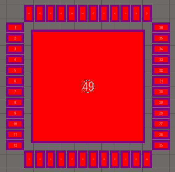
I am going to be using the DP83620 Ethernet PHY on my next product.  I downloaded the RHS package .bxl (UltraLibrarian) file from the TI website.  Using the UltraLibrarian Reader, I generated a footprint for Altium Designer.  The footprint is in the form of a script that you run in Altium Designer.  I ran the script and discovered it incorrectly generated the paste layer.  Here is a screenshot from Altium showing how the paste is shifted on each pad.  It looks the right size, just shifted.  I deleted the paste from pin 1 to show the pad underneath.

The solder mask looks correct, though one could argue it isn't because it violates minimum solder mask widths since the solder mask is only 1.7 mils wide in between the pads.  Technically it should ask what the minimum thickness can be, and what the default solder mask expansion is around each pad.  If the specs cannot be met, it should suppress the solder mask for the pads and generate a single solder mask rectangle around all the pads on a side.  But that is the way it should be in a perfect world.

I'm not sure where the problem is, but the reason for my post is not so much about the paste error above.  But I thought it would be good for someone at TI to know that this happened.

The main reason I am posting this is to find out where the footprint dimensions are decided.  Does someone at TI draw the footprint in the UltraLibrarian program?  Or does UltraLibrarian automatically generate footprints based on component dimensions?

I didn't see any guidelines for connecting the thermal pad to the ground plane through thermal vias.  Is there a recommended number of vias to the ground plane of a 4-layer board?

Please move this post to another forum if there is a more appropriate forum for this question.

Thanks and regards,

Greg

  • Please ignore what I said about the solder mask. It is only 1.7 mils because the default setting in Altium is set to a 4-mil expansion in the component editor. The expansion for each pad is set to default to the design rules setting.

    Something that might be helpful to know is that the paste expansion for each pad is set to -5 mils. Typically it is set to expand from the rules, which is typically the same size as the pad.

    Greg
  • Greg,

    We have an application note for this package family at:

    It includes some guidance on thermal vias. 

    Regarding your questions on the Ultra Librarian process, I will have to look into that and get back to you.

    Patrick

  • Hi Patrick,

    Thank you very much for pointing me to the application note! Besides the info on thermal vias, it explains the crazy stencil. I sure am glad I downloaded the .bxl file and generated the footprint. Thanks for looking into the Ultra Librarian process. I don't think there is anything wrong with its output. I'm going to guess that TI draws the footprints rather than Ultra Librarian calculating them on the fly. The dimensions mostly match the data sheet and application note. Would you please look at page 19 of the application note? The drawing on page 104 of the DP83620 data sheet says "SQA48A". The PCB pad size is the same as listed on page 19. But the stencil aperture in the Ultra Librarian footprint is exactly the same size as the pad (0.25 x 0.6 mm). But the app note says that is should be 0.25 x 0.7 mm.

    I am also using a TPS73701 in the design. Do you know if this appnote applies that the SON package or of there is an application note for the SON package?

    Thanks,

    Greg
  • Hi Patrick,

    I think I answered my question about the TPS73701. I found the application note for that type of package: www.ti.com/.../slua271a.pdf

    It doesn't look like the stencil is pushed out like it is with the LLP package type.

    Greg

  • One more thing I just remembered. The reason the paste expansion is set to -5 in each of the pads in the Altium footprint is because a negative number shrinks the paste expansion. In this case the X dimension of the pad is 10 mils, so the paste expansion needs to be -5 in order to shrink it to 0. Since the automatic paste generation is being suppressed, it needs to be manually drawn using a "Solid Region".

    Greg
  • Hi Patrick,

    I think we're pretty close to closing this case.  I understand what I need to do for the thermal vias, and why the paste is shifted on top of the solder mask.  But I don't know if I am to trust the application note or the footprint with respect to the size of the paste aperture.  The footprint has paste apertures that are identical to the pad, but the application note says they should be larger.

    Something I learned from the QFN/SON application note is that the side terminals are not plated.  This means a side fillet is not expected, which to me is frustrating because I don't get a good feeling about the quality of the solder connection.  I didn't see such information in the LLP application note about the side terminals not being plated, but the LLP application note points out that the No Pullback LLP allows for a fillet that improves reliability and inspection.  Do you happen to know if the side terminals of an LLP package are plated?  I'm just curious about the differences between LLP and QFN/SON since they seem to be very similar.  I'm wondering why the same trick of offsetting the paste aperture couldn't be used for SON as well.

    Thanks,

    Greg

  • Hi Patrick,

    The reason I am asking if the footprint or the application note is correct is because I am concerned that someone made a change to the footprint based on recent experience, but the application note was not updated accordingly.  Or it could be a mistake when someone created the footprint.

    It would be nice if the product page was updated with a link to the application note that you pointed me to.  It has a lot of good information in it.

    Thanks,

    Greg