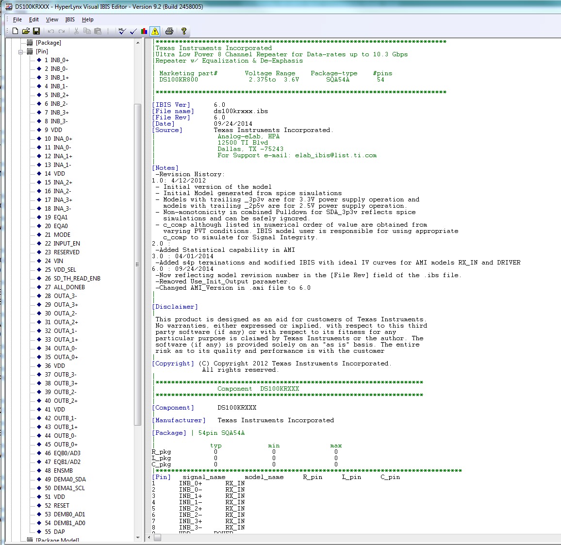
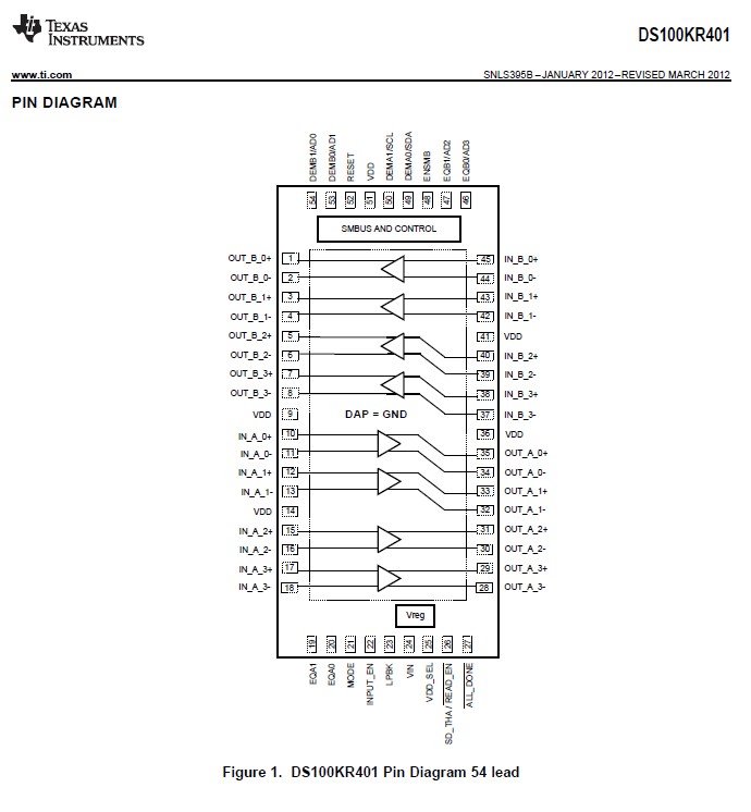
Hi, the IBIS model for the DS100KR401 shows pin 1 and 2 as inputs yet the datasheet shows them as outputs. Which one is correct? If the datasheet is correct, is it possible to get an updated IBIS model?
This thread has been locked.
If you have a related question, please click the "Ask a related question" button in the top right corner. The newly created question will be automatically linked to this question.
Hi, the IBIS model for the DS100KR401 shows pin 1 and 2 as inputs yet the datasheet shows them as outputs. Which one is correct? If the datasheet is correct, is it possible to get an updated IBIS model?
Hi Mike,
This model supports both DS100KR800 and DS100KR401. The primary pinout listed in the .IBS file is for the DS100KR800. I have highlighted the text changes below to remap the DS100KRxxx.ibs file to have the DS100KR401 pinout.
Regards,
Lee
Default Model Configuration DS100KR800 pinout
[Pin] signal_name model_name R_pin L_pin C_pin
1 INB_0+ RX_IN
2 INB_0- RX_IN
3 INB_1+ RX_IN
4 INB_1- RX_IN
5 INB_2+ RX_IN
6 INB_2- RX_IN
7 INB_3+ RX_IN
8 INB_3- RX_IN
37 OUTB_3- DRIVER
38 OUTB_3+ DRIVER
39 OUTB_2- DRIVER
40 OUTB_2+ DRIVER
42 OUTB_1- DRIVER
43 OUTB_1+ DRIVER
44 OUTB_0- DRIVER
45 OUTB_0+ DRIVER
[Diff Pin] inv_pin vdiff tdelay_typ tdelay_min tdelay_max
|
1 2 200mV
3 4 200mV
5 6 200mV
7 8 200mV
38 37 NA
40 39 NA
43 42 NA
45 44 NA
|
Changes to Model Configuration for DS100KR401 pinout
[Pin] signal_name model_name R_pin L_pin C_pin
1 OUTB_0+ DRIVER
2 OUTB_0- DRIVER
3 OUTB_1+ DRIVER
4 OUTB_1- DRIVER
5 OUTB_2+ DRIVER
6 OUTB_2- DRIVER
7 OUTB_3+ DRIVER
8 OUTB_3- DRIVER
37 INB_3- RX_IN
38 INB_3+ RX_IN
39 INB_2- RX_IN
40 INB_2+ RX_IN
42 INB_1- RX_IN
43 INB_1+ RX_IN
44 INB_0- RX_IN
45 INB_0+ RX_IN
[Diff Pin] inv_pin vdiff tdelay_typ tdelay_min tdelay_max
|
1 2 NA
3 4 NA
5 6 NA
7 8 NA
38 37 200mV
40 39 200mV
43 42 200mV
45 44 200mV
|