This thread has been locked.

If you have a related question, please click the "Ask a related question" button in the top right corner. The newly created question will be automatically linked to this question.

HD3SS460 / typical application (Figure 8.)

Guru 29720 points
Other Parts Discussed in Thread: HD3SS460

Hi Team,

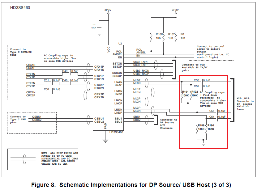
Does the following Figure 8. shows "AC Coupling cap + Pull-down resistor" is required for ML0P/N and ML3P/N only?
I believe it is just omitted and "AC Coupling cap + Pull-down resistor" is also required for ML1P/N and ML2P/N.

Is my understanding correct?
I would like to confirm just in case.


Best Regards,
Yaita / Japan disty

  • Hello Yaita-san,

    The figure is right, you only need the biasing resistors and caps on two lanes because the schematic corresponds to the DP source (2 lanes) + USB3 configuration.

    Please refer to the table 1 to confirm which lanes must be biased & AC coupled for the customer's application.

    Regards,
    Diego.
  • Hi Diego-san,

    Thank you for your support.
    I understood Figure 8. shows  DP source (2 lanes) + USB3 configuration.

    Which configuration(POL, AMSEL, EN) in Table 1. is selected in Figure 8.?
    I tried to catch it, but couldn't.

    Your support would be appreciated.

    Best Regards,
    Yaita / Japan disty

  • Diego-san,

    May I have your advice about the follwoing issue? 
    >Which configuration(POL, AMSEL, EN) in Table 1. is selected in Figure 8.?

    Best Regards,
    Yaita

  • Hello Yaita-san,

        Seems to be the first two options from the tabe but with a Typo (LANES A & B instead A & D).

    Regards,

    Diego.

  • Hi Diego-san,

    I appreciate for your support.

    Could you modify the datasheet in next revision?
    I think it is critical if customer will design the schematic same as Figure.8.

    Best regards,
    Yaita

  • Diego-san,

    I still wonder if Figure 8. only corresponds to "DP source (2 lanes) + USB3" configuration.
    I believe Figure 8. is applicable to another configuration in table1, for example "4CH AM" in DP-Source/USB-Host application.
    Could you clarify above?

    Your support would be really appreciated.

    Best Regards,
    Yaita

  • Top 4 configurations in the table 1 can be supported with the connection shown in the Figure 8.  The DP Alt mode over Type-C specification requires the AC coupling capactors to be placed on the other side of the Type-C connection(the Type-C pins where the CRX1 and RX2 pairs are to be connected in Figure8), therefore the placement of the AC caps and the pull-downs on ML0 and ML3 are optional.  

  • Hi Yoon-san,

    Thank you for your support.
    I would like to ask additional two questions.

    1)
    >Top 4 configurations in the table 1 can be supported with the connection shown in the Figure 8.
    If Top 4 configuration can be supported as you said, I believe the other configuration can also be supported because internal path of HD3SS460 seems the same.
    Is my understanding correct?
    If the answer is no, why the other configuration can't be supported?

    2)
    I understood "4CH AM" can be supported with the connection shown in the Figure 8.
    Why does the Figure 8. show "AC Coupling cap + Pull-down resistor" for ML0 and ML3 only although "4ch AM"?


    3)
    I understood the placement of "AC Coupling cap + Pull-down resistor" on ML0 and ML3 in Figure 8. are optional.
    Could you tell me the criterion to decide to put them?

    Best regards,
    Yaita / Japan disty

  • Please refer to the table below.  The HD3SS460 connection shown in the example figures are intended to support source(DFP_D) pin assigmnet C, D, E and F and sink(UFP_D) pin assignment C and D.  The ML lane 0 and 3 are connected to RX pins on the source side which will be connected TX pins on the sink side with a Type-C cable connection, .  Per the DP Alt mode over Type-C requirement, the TX pins must have AC coupling capacitors between the mux switch and the USB-C connector therefore the capacitors on the ML0 and 3 shown in figure 8 can be removed.  The capacitors and pull-downs were added at an early phase of the Alt mode adoption as some vendors did not follow the spec requirement for the AC coupling cap placement.  Please refer to the DP over Alt mode spec for details on this requirement.    VESA member company employees should have access to the spec at VESA.org.

  • Hi Yoon-san,

    I really appreciate for your kind support.
    I understood.

    Best Regards,
    Yaita

  • Hi Yoon-san,
     
    My customer saw "DP over Alt mode spec" however he couldn't convince the capacitors and pull-downs on the ML0 and 3 shown in figure 8 can be removed.
    I believe it is better to implement the capacitors and pull-downs on the ML0 and 3 shown in figure 8 because DP sink application that is connected over typeC doesn't need to implement AC coupling cap.
    What do you think about it? May I have your comment once again?

    Best Regards,
    Yaita

  • please see (page 27 of the spec version 1.0a).  The pin configuration represented in Figure 8 is intended to support pin assignment C, D, E and F for DFP_D systems.  The ML0 and ML3 map to pin number A10-A11, B10-B11, therefore the AC capacitors will be present on the other side of the connection(SSRX connects to SSTX via the cable connection).  It is required for the plug based adapter to include AC capacitors on pin A10-A11, B10-B11 as stated in the spec reference above.