This thread has been locked.

If you have a related question, please click the "Ask a related question" button in the top right corner. The newly created question will be automatically linked to this question.

Trouble with SN65LVDS310

Hi,

We're working on a project with very tight space constraints, and are in need of a SER/DESER solution to carry data from our Artic7 FPGA. Given the space constraints, we are looking to use the Artic7 as a SER and connect 2 of its LVDS outputs directly to a SN65LVDS310.

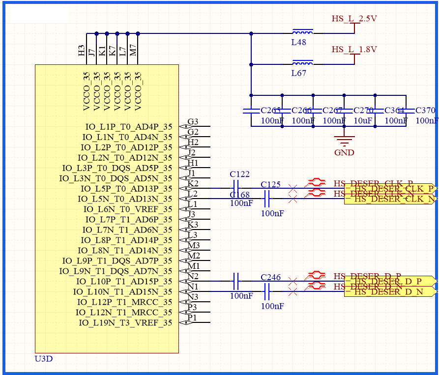
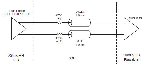
There is a potential problem of LVDS<>SubLVDS mismatch, but based on Xilinx' xapp582 we decided to invest time in a small testboard (since devkits are not available and our local rep couldn't get us anything similar). xapp582 advises to put series resistors close to the transmitter, which we did to get the signals within the recommended operating range of the SN65LVDS310.

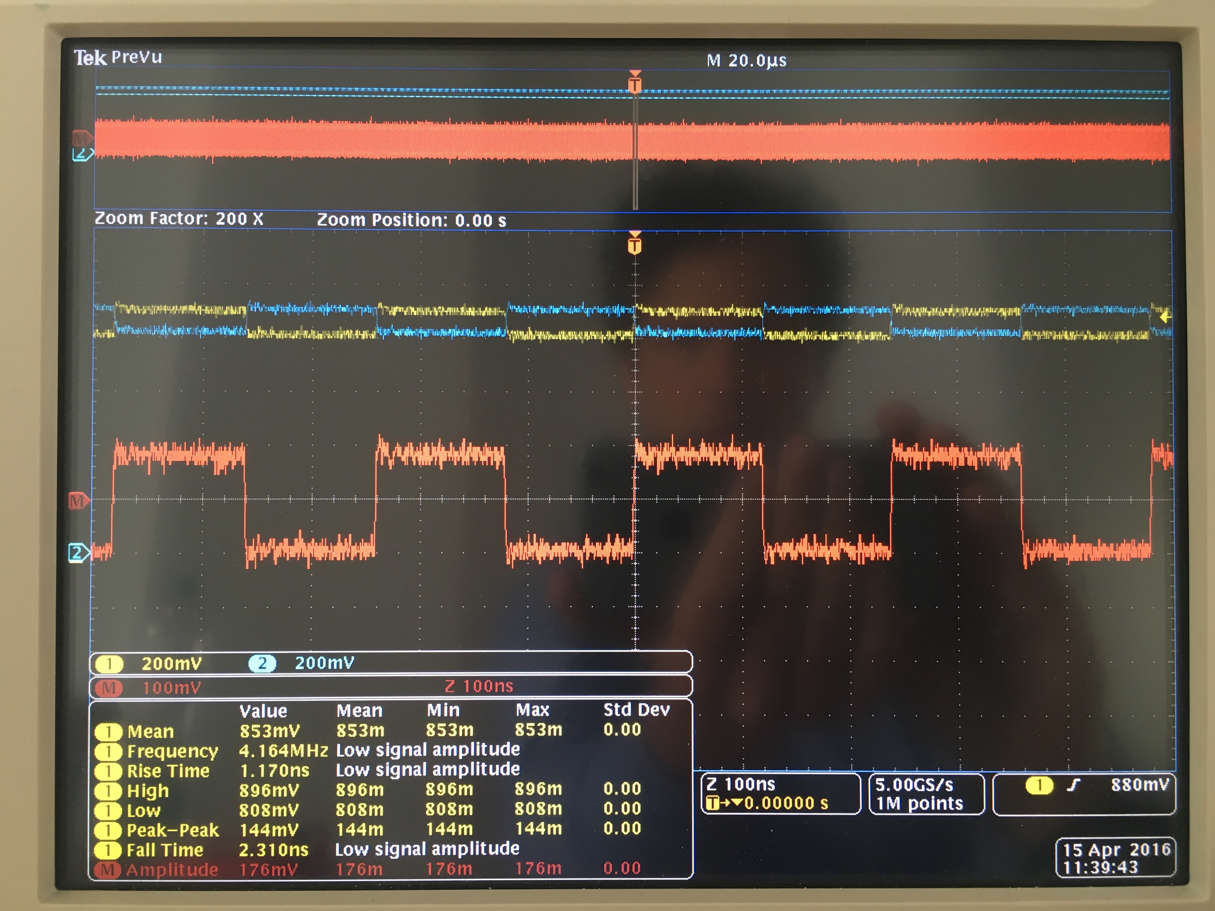
Below is a screenshot of how what the 4.167MHz clock signal towards the SN65LVDS310 looks like. Yellow/blue are the CLK+/-, red is their difference, indicating a 176mV differential amplitude, well within the 70mV-200mV range specced in the SN65LVDS310 datasheet. (measure using 1GHz passive probes on 1GHz bandwidth scope, 1MOhm termination)

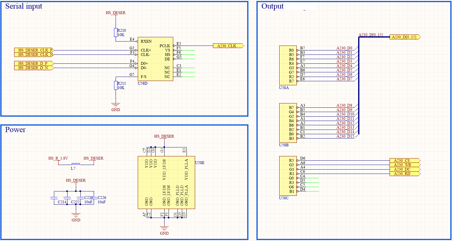
However, the SN65LVDS310 is not reacting at all. Regardless of the Data lines (which are presenting a fixed value at the same voltage levels as the clock), we believe the SN65LVDS310 is supposed to produce a 4.167MHz clock. But the clock output is staying low, as well as DE; while other outputs are high. (most signals connector to other non-driving ICs; while the clock output is floating)

Can you please recommend how we should attempt to get the output clock running?

Additional information:

- Stable 1.78V on all supply pins (All VDD types shorted together)

- RXEN pulled up to VDD using 10Kohm (1.78V on RXEN side)

- F/S pulled down using 10Kohm

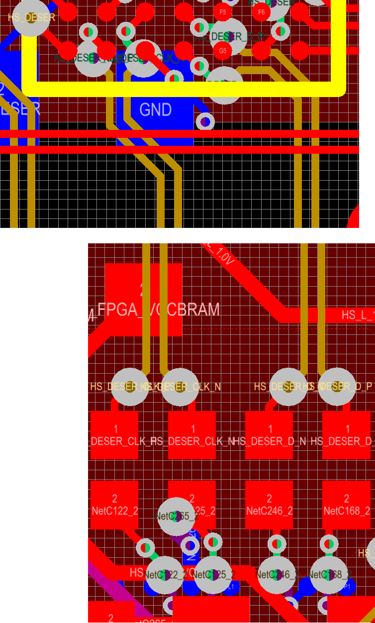
- Traces between transmitter resistors and receiver routed as 100ohm diffpair, 3cm runlength (see below)

- No termination resistors used at receiving side (as they are assumed to be internal) (see below)

  • Hello,
    If PCLK and DE are static low that means the device is not receiving a valid input clock, what is the DC level on the input clock?
    The device could be going to stand by mode.
    Can you share your schematic?
    Regards
  • Thanks for the reply.

    1/ The CM voltage on the input signals is around 850mV (see the scope screenshot above for more detail)

    2/ Schematic details below.

    FPGA first, where we have a full bank dedicated for these output signals (so we can play with voltage levels)

    Please note that these cap footprints have been fitted with 470ohm resistors.

    Schematic of the SN65LVDS310:

    Any comments/questions/suggestions welcome.

  • Hello,

    Have you tried with more than one unit.
    Regards,
    Diego.
  • Diego,

    Indeed, we have 4 boards at our disposal; all show the same behaviour.

    One more element: the waveforms above were probed on the resistors close at the FPGA, so before the 3cm 'transmission line'. We cannot probe the signal close to the receiver. But with a 4MHz clock running over 3cm, I believe this should not be an issue.

    Is it correct that the state of the datalines have no influence at all on the generation of the output clock? Even though they carry signals of the same voltage levels as the input clock, the data probably fails the CRC check.

  • Riemerg, I took a quick look.  It's not clear what the problem is.  One thing you could check is Icc: does it match active, standby, or shutdown mode?  Does disabling the clock have no effect on Icc?

    Next, can you increase the clock VID or its frequency to see if that fixes it?  I think you can exceed 200mV without problem.

    Best regards,

    RE

  • RE,

    Thanks a lot for your reply and suggestions.

    1/ Voltage level

    We've tried applying larger voltage swings, but the result stays the same. We even went to 1Vpp, so 2Vpp differential. The measurements below were done with resistors resulting in 260mVpp differential, so 130mVpp single-ended, on a 850mV common mode.

    2/ Frequency - Current

    Unfortunately, the PCB allows us only to measure global current consumption.

    Below the combined current consumption based on some clock variations:

    Clock off (both entries at 1.8V): 0.986mA

    4.125MHz clock: 2.529mA

    6.667MHz clock: 2.533mA

    10.000MHz: 2.538mA

    Looking at a shutdown spec of 0.01mA and standby spec of 0.1mA, it seems the chip is in Acquire or Receive mode. Not sure which one of them?

    3/ PCLK output pin

    When we first power the device and leave the clock inputs floating, the device presents a 46.6mV voltage on the PCLK pin. As soon as we start driving the input clock, the PCLK seems to be forced to 0V.

    Of course, any other suggestions/thoughts are very welcome!

    We have the opportunity of a respin of the same board beginning of next week, so feedback is very much appreciated.

  • Regarding 3/ PCLK output pin:


    The PCLK pin (as well as all other connected output pins of the SN65LVDS310 in the schematics above) is looped back to the FPGA. Hence, the 46.6mV will probably be caused by the pull-up of the FPGA when it's unconfigured. Once configured, the FPGA floats all of the SN65LVDS310 outputs.

    So we're not sure the SN65LVDS310 is really changing the state of PCLK when presented with a clock.

    However, the PCLK is low, while its other outputs are high, while all of them are treated the same (floated) by the FPGA.

  • Hi riemerg,

    Can you try toggling RXEN to see if that changes current by 0.015mA?  That's the difference between standby and shutdown mode (per the datasheet).

    Quite simply, "A high input signal on RXEN combined with a CLK input signal switching faster than 3 MHz and VICM smaller than 1.3 V forces the SN65LVDS310 into the active mode."  If there is no PCLK output, then something unexpected is wrong.  Check connections, and verify the schematic.

    Best regards,
    RE

  • None of our multimeters allow me to make a 100% stable measurement, so don't trust the following figures blindly. There is an increase in current, when I switch RXEN from GND to 1.8V. This is about 0.2mA when no clock is applied, and about 1.5mA when a 6.6MHz clock is applied.

    The IC is indeed quite simple. That's why I'm turning to this forum as we're getting a bit clueless. Schematics seem OK (see above), and the footprint corresponds to the datasheet. We have other 0.5mm BGAs soldered on the board which work just fine.

    The best would be to have some kind of evaluation board, so we have a working sample with which we can experiment. Our distributor (Avnet) says this is not available, but some kind of PCB must exist? It would be hard to believe a chip is launched without having it ever soldered to a board before :)
  • With this issue still not being solved, we received support from TI by mail, so I list the communication below to keep this thread updated:

    The only issue I can imagine is  soldering issue or improper connection of the pins and GND.

    4 boards show exactly the same behaviour, other 0.5mm pitch BGAs on the same board are working flawlessly. 
    Pinout has been triple-checked by different persons against http://www.ti.com/lit/ds/symlink/sn65lvds310.pdf
    Nevertheless, we've ordered a respin of this batch with specific attention to this IC, to sort out any potential soldering issues.
    Can they connect an external clock generator to CLK+, CLK- pins with recommended levels?
    With the current board, we can already change the amplitude and common mode of the clock signals, yet we cannot get the chip into Receive mode.
    See the screenshots on E2E to see 2 configurations which are withing specs of the datasheet.
    We would of course be willing to hook up an external clocking device, however could you advice which IC should certainly work?
     
    Meanwhile, I will check if someone at TI has an EVM so that customer can make some tests on a known good HW.
    This would be appreciated the most, as it would undoubtly lead to a solution.
    Or for the time being, a screenshot of the waves arriving at the IC on a working setup (like I posted on E2E), so we can try to mimic these 100%.
  • Dear TI engineers,

    This might be the last post in this thread. If it it not possible to provide us with an evaluation module, or at the very least with a screencapture of the input waveforms of a working setup, we will be forced to use an alternative part from a different vendor. At this point, this chip is the only remaining hardware issue we have on this project.

    Regards,

    Riemer

  • Hello,
    I apologize for the negative experience you've had, I'm still trying to get you an EVM, would it be possible for you to ship one of your board to us for debug?
    Regards
  • Elias,

    Thanks for the offer, I hadn't yet though about this opposite approach approach, but it could obviously work as well.

    Would it be possible to contact me at riemer (dot) grootjans (at) gmail (dot) com? Afterwards I will contact you through my working mail to discuss the practical details.

    Regards,

    Riemer

  • Dear TI engineers,

    With this SN65LVDS310 problem still existing, and TI not able to send us a working EVM, we even created our own PCB with a SN65LVDS310 deserializer fed by a SN65LVDS307 serializer. Sending a 5MHz clock to the SN65LVDS307 results in valid CLK+- and D+- signals being generated, but the SN65LVDS310 still refuses to react: PCLK output is low, all data outputs are pulled high.

    Connectivity has been checked over and over again, we have the problem persisting on multiple boards on multiple designs. Would it be possible to send this board to you so you can create your opinion? Please contact me at the mail address provided in the previous post.

    Regards,
    Riemer
  • Dear TI engineers,

    Would it be possible to provide a short answer? The functionality of our current design is severely limited because of this issue.

    Regards,

    Riemer

  • Dear TI engineers,

    Any update please?

    Regards,

    Riemer

  • Sorry for the delay,
    We are analyzing the debug capabilities, are you able to ship a complete set up to Dallas for debug?
    Regards
  • Elias,

    Thank you for the reply.

    That is correct; we have a board ready to be shipped to you once we get the shipping address. Please contact me on the mail address I provided earlier, so I can already share all details about the board.

    Regards,

    Riemer

  • Elias,

    I haven't yet received a mail from you.

    Please send a message to riemer (dot) grootjans (at) gmail (dot) com, after which I will contact you from my working mail in order to get the board to you asap.

    Regards,

    Riemer

  • Elias,

    Can you please give me an update regarding how to get to a solution? I have far too many positive experiences with TI to give up on a chip like this. All I'm asking is to send me a mail, so I can share all details regarding the non-working 307+310 combination we have. Preferably an address as well, so we can look at the same type of board.

    Regards,

    Riemer

  • Hello,

    Sorry for the long delay, at this moment it will be impractical to receive your board.

    We talked with the Tech champion and this is what we think is going on:

    They attenuation is such that the common mode below 0.9 X VDD LVDS

     It will put the device into standby mode and kill the output.

  • Elias,

    Apologies for the delayed answer, in the meantime we asked for and received a FIN424/FIN425 ser/deser devkit from Fairchild which is working quite fine.

    However, since our current protos have the SN65LVDS310 implemented and this is a better (smaller) fit for our smartglass , I would still very much prefer to get this IC working.

    That being said, can you please ask your tech expert to have a quick look at my original post, where you can clearly see the common mode is at 850mV, which is well below 0.9*VDD = 1.62V.

    At this moment, I'm thinking we're dealing with bad silicon (even though these parts originated from Digikey). Is there a way you could get validated silicon to us fast? So we can replace the component on the boards. I would like to check this asap, as we'll need to make the call between FIN425 and SN65LVDS310 soon (redesign is currently planned next week).

    Regards,

    Riemer

  • Hello,
    I have forwarded this requirement to my product manager.
    They shall contact you shortly.
    Regards
  • Have you started a FA request for the suspicious parts?
    Regards