This thread has been locked.

If you have a related question, please click the "Ask a related question" button in the top right corner. The newly created question will be automatically linked to this question.

Troubleshooting HDMI video through TS3DV642 (part 2)

Other Parts Discussed in Thread: TS3DV642, TPD12S016

This is a continuation of a post I made a month ago here. In summary, I had used a TS3DV642 in a design that needed to switch two sources to one sink. I was never able to see the source's video on the sink display and never really got to the bottom of the problem. I just assumed it was a PCB layout issue. https://e2e.ti.com/support/interface/etc_interface/f/388/t/505473

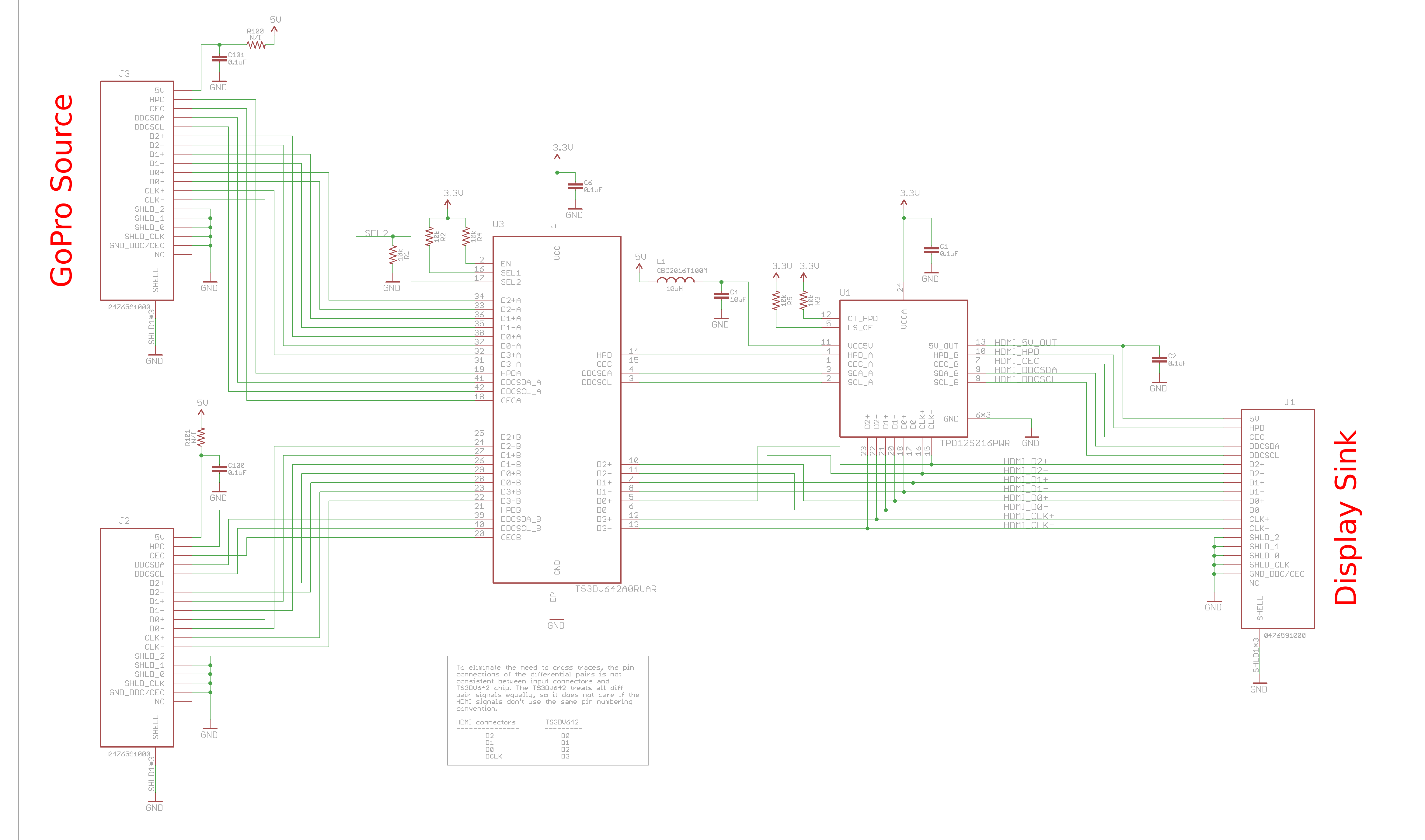
I designed a new PCB and removed everything on the board I didn't need. I went to great lengths to length match and impedance control the differential pair traces, so I no longer have any concerns that the PCB layout itself is the problem. My new schematic is copied below. Unfortunately, I'm running into the same issue still: no video on the display.

Here's the troubleshooting steps I've tried so far. I have a GoPro plugged into J3 (channel A on the TS3DV642) and a HDMI display monitor plugged into J1. The SEL1 and SEL2 pins are pulled-up and pulled-down, respectively, to use channel A.

1. I confirmed that the display monitor works with the GoPro when the GoPro is plugged directly into the display. Therefore, I know the display is compatible with the resolution and framerate of the GoPro.

2. I confirmed the HDP signal is getting all the way from the sink connector to the GoPro's connector. It sits at about 4V when the display is attached.

3. I removed the TPD12S016PWR chip, which is an ESD and I2C buffer chip, just in case it was causing the problem. Consequently, I had to green-wire the HPD, DDCSDA, and DDCSCL pins directly from the sink connector (J1) to the TS3DV642. I assume the CEC signal is not required for personal devices like a GoPro, so I left that one floating.

4. I added pull-up resistors to 5V on the DDCSDA and DDCSCL signals on the GoPro side. In other words, I soldered 2k pull-up resistors to the I2C lines coming directly off of the J3 connector.

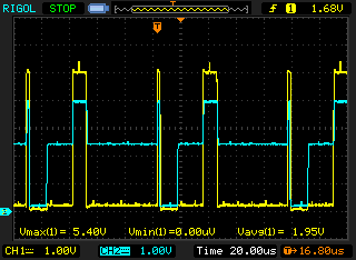
5. I confirmed the I2C comms is getting all the way from the GoPro to the sink connector using my oscilloscope.

Unfortunately I don't have access to an oscilloscope that is fast enough to probe HDMI, so I can't probe the HDMI signals themselves. I've tried multiple displays and they all do the same thing: absolutely nothing. I would expect errors or "Resolution Not Supported" or similar messages, but they don't seem to notice that anything is plugged in at all. In fact, one of the displays I tried actually tells you what device it detected that you plug it in. So when I plug the GoPro directly into the display (without my circuit), it correctly shows "Input: GoPro Hero4". When I use that exact same GoPro in my circuit, the display fails to detect the GoPro at all.

I'm happy to share my entire schematic and PCB layout if that would be helpful to anyone. It's in Cadsoft Eagle. I'm still assuming there's something very basic about my design that is causing the problem. Any thoughts and troubleshooting advice would be very helpful!

  • I think I found something interesting. I probed the DDC SDA lines at both connectors.  The sink (HDMI display screen) side looks pretty good. The square waves travel between 0V and 5V fairly cleanly. The source (GoPro) side, however, looks bizarre. It moves between 0V, 2.5V, and 4V. To me, it looks like there's a resistor divider being formed somewhere. See the screen shot from my oscilloscope below. Yellow trace is SDA at the sink connector. Blue trace is SDA at the source connector.

    Could this be some unintentional effect from the TPD12S016? Since the GoPro is a fully integrated consumer electronic device, it must already take care of the pull-up resistors on the I2C line, right? I wonder if the TPD12S016 is just complicating things because it has its own pull-ups. Any thoughts on this?

    Yellow: SDA at sink (HDMI display)
    Blue: SDA at souce (GoPro)

  • Daniel,

    Without being able to probe the signal paths of the signal switch I don't see any issue with your TS3DV642.

    I have someone on my team that has some experience with HDMI and I have forwarded this thread to him to take a look.

    I will also move this thread over to the ESD forum for comment on the TPD12S016

    Adam
  • Adam,

    Thank you. Please let me know if the HDMI guru you know has any insight.

    -Dan

  • Hi Dan,

    Does the TS3DV642 have built in pull-ups on the DDC output? If so (and I suspect so), that is causing this issue. Can the pull-ups in TS3DV642 be disabled?

    Regards,
  • Guy,

    To my knowledge, the TS3DV642 does not. I just went through the datasheet again and did not find any reference to internal pull-ups.

    -Dan Laks
  • Guy,

    Daniel is correct, the TS3DV642 does not have any internal pull ups. The device is a bi directional passive FET switch.

    Adam
  • Hi Dan,

    Okay then, no external pull-ups is a good thing. Let me be sure: In the oscilloscope waveform above, is the "SDA at source" measurement on the system side (A-side) of TPD12S016? For now I will assume the waveform is the A-side.
    I notice that VCCA=3.3V, so the A-side should pull up to 0.8( VCCA), but it looks to be pulling up to 4V.

    Is it possible I can see SDA on both the A-side and B-side?

    Thanks,
  • Guy,

    I was actually referring to the HDMI connectors themselves when I wrote "source" and "sink" in my previous posts. I was probing the SDA pins on the HDMI connector going out to the display (sink) and the same pin on the connector going out to the GoPro (source).

    Even though the TS3DV642 doesn't have any internal pull-ups, I'm pretty sure the GoPro and/or the display does. And apparently so does the TPD12S016. The 4V I was getting was almost certainly a resistor divide between 5V and 3.3V. I still don't know where the 2.5V was coming from.

    I've been testing a lot of things since yesterday and have ultimately bypassed the I2C port entirely. In other words, I've green-wired the SDA and SCL lines directly from HDMI connector to HDMI connector. I kept the TPD12S016 chip on the board, but I lifted the SDA and SCL pins off the pads so they don't influence the I2C comms at all.

    So now the I2C comms should have a direct, unmolested connection between the display and the GoPro. Still no video though. Unfortunately I can't probe the A and B sides now as you requested because I've lifted those pins, but I think that's no longer relevant because I've bypassed the TPD12S016 anyway.

    -Dan

  • Hi Dan, Adam,

    If the source has pull-ups then there should be the same issue because it will be a low impedance path through the TS3DV642 (please confirm that Adam). So I think your approach is a good one: bypass the DDC past TPD12S016 to try and get the EDID exchanged and once that works, then see if the pull-ups between the TVS and the Source are a problem.

    With the bypass in place, have you taken a waveform of SDA yet?

    Regards,
  • I have and it's not what I expected. Now both SDA and SCL are just idling high and do nothing. No trigger I can set up seems to catch any comms at all.

    I've confirmed that the SDA and SCL lines are continuous from connector to connector and the green wires are not shorting together or to any neighboring traces. Now I'm just confused...
  • Whoops, ignore my last post. Now it's working!

    It appears the HDMI connectors I'm using on my PCB are maybe not the highest quality. When I wiggled the cable in the connector a little, suddenly the display sprung to life and is showing video. I can make the video go in and out by just tilting the cable back and forth. I'll have to source some better connectors going forward.

    Anyway, it seems there was definitely a conflict using the TPD12S016 with a GoPro. I think I understand now that the TPD12S016 was designed for "raw" video sources that don't already have the required pull-up resistors and such. A fully integrated commercial product like a GoPro will just conflict with it.

    Thank you Guy and Adam for your help with this!
    -Dan
  • Hi Dan,

    Great! Now ... I am pretty sure that the GoPro Source pull-ups on the DDC outputs can be disabled, and I recommend using the TPD12S016 with it. I see that TS3DV642 offers only 6.5 ohms of Ron, so any pull-ups on the other side of it will still reduce the ability of the TPD12S016 to pull down the A-side, basically lowering the VOL of the A-side translators.

    I am glad you got it working. Please let me know if you have any other questions.

    Best Regards,

  • Guy,

    How would you go about disabling the pull-ups on the GoPro? I wouldn't think that would be configurable.

    -Dan
  • Hi Dan,

    I am not sure how to address the GoPro source and disable the pull-ups. I would have to refer your to their documentation and support.

    I had another question come to mind: When you blue wired the DDC past TPD12S016, what logic level is the HDMI source working at? The Sink should see 5V, but I believe your Source is lower than that without the PD12S016.

    Regards,

  • Guy,

    Oh sorry, I misinterpreted your previous message. I thought you were saying you knew it was possible to disable the pull-ups on a GoPro.

    It looks like the source is pulling the I2C lines up to 5V. I suppose that's not a surprise because you can plug a GoPro directly into an HDTV with an HDMI cable and it will display the video. No level shifting required.

    -Dan