This thread has been locked.

If you have a related question, please click the "Ask a related question" button in the top right corner. The newly created question will be automatically linked to this question.

The PCA9306 describe difference between 2014's version and 2016's version

Other Parts Discussed in Thread: PCA9306

Hi Sirs

I have a question about PCA9306's describe difference between 2014's version and 2016's version.

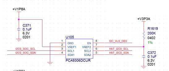
Please refer below figure. Which one is right for PCA9306?Please help me to explain it. Thanks.

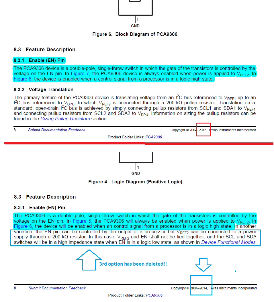
My design is EN and VREF2 isn't connected together and the EN pin >= 1 voltage than VREF1, then SCL2 & SDA2 is 3.3v level .

If the En pin more than 2.8v ( 1v + 1.8v VREF1 ), the SCL2 & SDA2 will be 2.2v level.

Thank you for your great support.

  • Hi Hugo ,

    I will move this into the I2C forum for support .
  • Hi Hugo,

    Thanks for the question.

    The correct version of the PCA9306 datasheets would be the 2016 version which has omitted that 3rd option you are referring to. Before I get into the corrections that should be made to the schematic, I'll explain the reason for the change. The main reason for the change was that this was due to the confusion of that option. Something to consider when designing with PCA9306 is that this device is a level translating I2C switch, which means that each switch is turned on with the EN pin. With these internal switches, we need to ensure that we have a VGS higher than the threshold voltage of 0.8V to have the switch turn on. Which means that it's better to have the EN tied to VREF2. Without having the EN tied to VREF2, you run the risk of losing your translation of VREF1 to VREF2 by having the switch not turn on.

    Now for the suggestions for changes in schematic: 

    My main suggestion would be to short EN to VREF2, and instead of having V3P3A as your supply voltage, merely change that voltage to your I2C_VLS_OE0.

    Hope this helps!

    Siby