This thread has been locked.

If you have a related question, please click the "Ask a related question" button in the top right corner. The newly created question will be automatically linked to this question.

TUSB1310A does not data lock -X TAL oscillator jitter requirements?

Other Parts Discussed in Thread: TUSB1310A

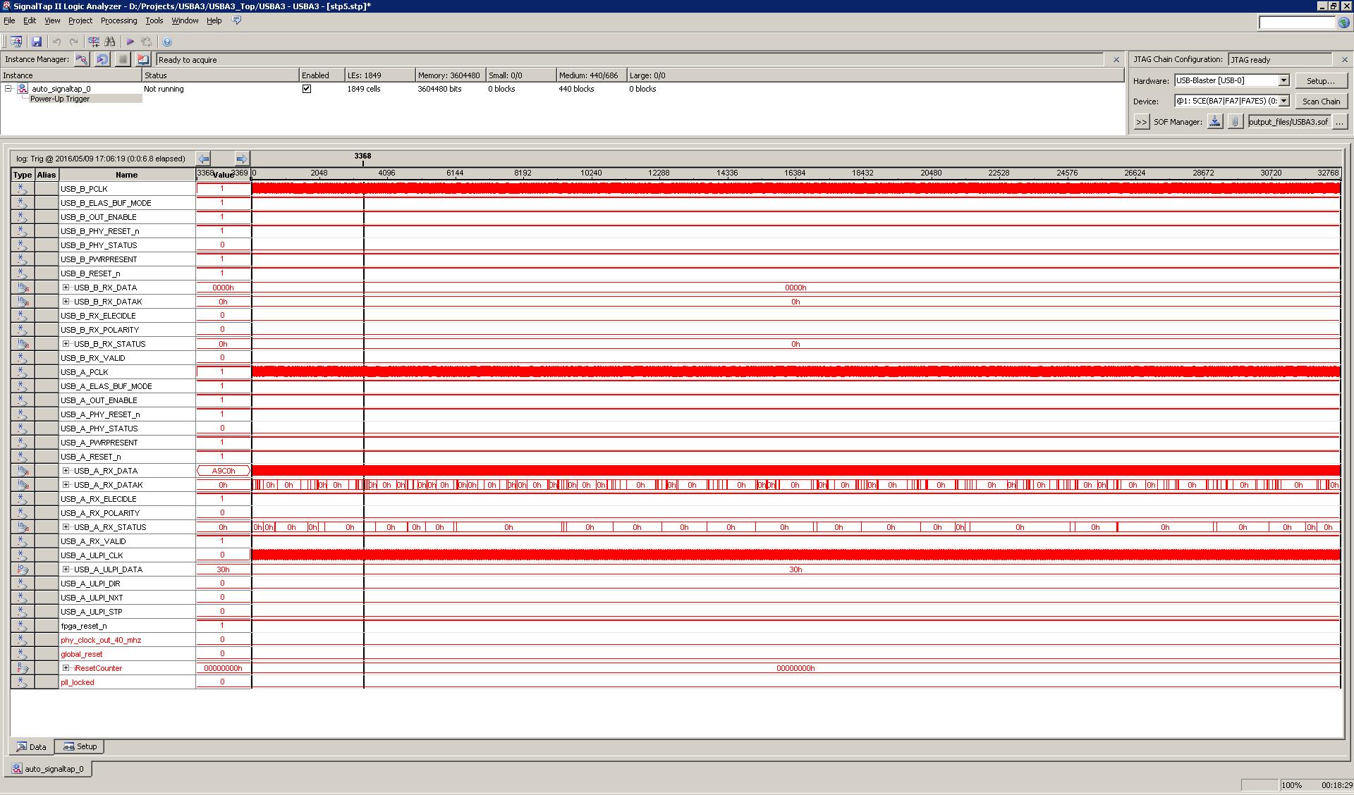
I have two TUSB1310A on my board (USB 3.0 protocol analyzer design). Both reset fine and de-assert PHY_STATUS. Both output 250 MHz PCLK and both detect LFPS fine. Scope shows good eye diagram at both SSRX pins. However, only one of the PHYs actually lock onto data (PHY A). The other one (PHY B) only de-asserts RX_ELECIDLE and never passes any RX data.

I have measured the oscillator cycle-cycle jitter (external 40 MHz XTAL) and get the below results. This is measured across the XI/VSSOSC capacitors:

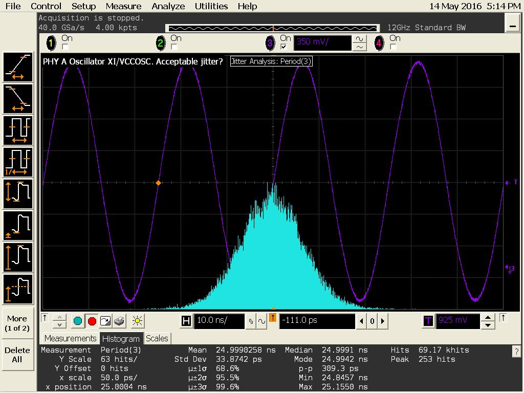
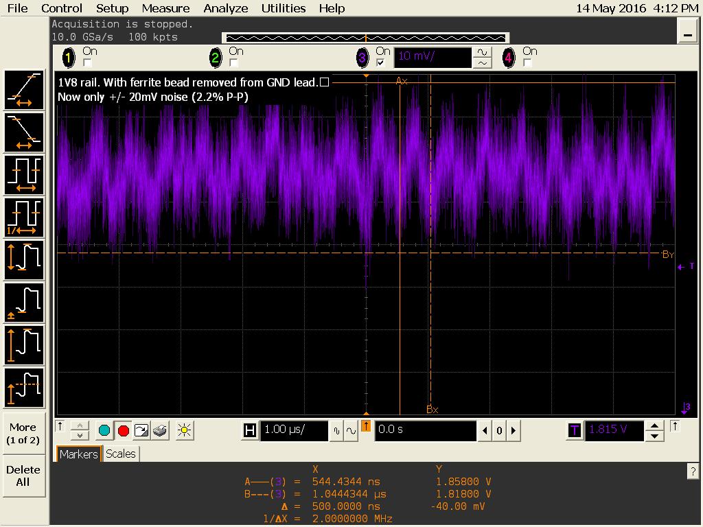
My scope shows the p-p jitter around 300ps. Is this too high? The datasheet says that an external oscillator should have "absolute p-p" 50ps or less but what about the built-in oscillator? The 1.8V power rail to the TUSB1310A is quiet, with about 40mV p-p per below scope screen shot.

If the jitter is too high, what specs should I use? 1 sigma, std deviation or max p-p? What jitter should PCLK have? Too high (due to power supply noise, for instance, could interfere with data lock?).

Thank you.

/John

  • Here are some supporting information I got from my spectrum analyzer. We can see the 2 MHz switching frequency of the switched mode regulators having about 50mV amplitude (p-p), which is about 70 dBm lower than the main 40 MHz oscillator frequency. I suspect that the non data lock may be that the noise level of the 1.8V supply rail is too large and couples too much into the oscillator, causes trouble for the CDR in the TUSB1310A. The current board revision does not have separate analog power rails for the TUSB1310A so the switching noise goes straight into the oscillator and PLL. Can you check with the designers how much noise is acceptable on the analog supply pins? When redesigning the board, I need to know how noise free the 'analog' power pins need to be.

    Also, there are "analog" 3.3V, 1.8V and 1.1V power pins as well as separate analog GND pins. Do these all need to be isolated via ferrite beads? What is the noise requirements on these power rails?

    Thanks,

    /John.

  • I have changed the 1.8V power to an external power supply. The switching noise is gone and I would now like to validate the phase noise in the generated 40 MHz oscillator to make sure it performs as expected. Could you please state what the maximum acceptable phase noise [dBc/hz] of the oscillator must be for the PLL and CDR to lock properly? I have measured and calculated -95 dBc @ 10 KHz.

    Please see following for supporting information:

  • I have now read in on the various methods of measuring jitter and I believe what the TUSB1310A datasheet specifies as "absolute reference clock phase jitter  (p-p) = 50ps is the same thing as Time Interval Error (TIE) jitter measured on an oscilloscope. Measured on my scope (between XI/VSSOSC) I get 26ps p-p TIE jitter. Can TI confirm that this is correct and that the oscillator clock is good?

    If the oscillator clock is good, why can't the PHY data lock? Also, can use of SSC interfere with data lock? What else to check?

    Thanks,

    /John.

  • Hello John,
    Sorry for the long delay. we will reply as soon as possible.

    Regards,
    Gerardo
  • Hello John,

    The noise requirements for power pins3.3V, 1.8Vand 1.1V are:

    Ripple of +/-30mV up to 20MHz

    Ripple of +/-20mV above 20MHz

    Regards,

    Gerardo