This thread has been locked.

If you have a related question, please click the "Ask a related question" button in the top right corner. The newly created question will be automatically linked to this question.

LIN communication through SCI to SN65HVD1781-Q1 pin 1 R

Other Parts Discussed in Thread: SN65HVD1781

I am able to transmit data through this device on a LIN TX comm line to a TMS570 Champion micro, but I am not seeing the data on the R pin of the device. I know the code works because I tested the SCI communication by itself through a loopback. Do I need a pull up resistor to receive data on this pin? Is there an application note which shows data being transmitted or received through this device? I may need an example.

  • Hi Infane,

    The SN65HVD1781 is an RS-485 transceiver and not a LIN transceiver, I am a little confused over what your architecture is. Can you help me understand the overall architecture better? For example: micro to LIN bus or micro to RS-485 bus or micro to a hybrid bus using the two different physical layer standards?

    LIN is a single ended signal that is driven from a micro into pin 4 of the transceiver and out of pin 6 of the transceiver. The pin 6 output (LIN output) can range from 9-30V in amplitude. RS-485 comes into the transceiver single ended from a micro like LIN but it leave differentially through pins 6 and 7 with a 2.5V common mode and 2V Vod.
  • Hi Michael, its a micro to LIN bus. We have data coming in through pin 4(D) and data going out from pin 1 (R). RE is tied to ground and DE is tied to VCC. On the data sheet. Pin 1 is R, pin 2 is RE, pin 3 is DE, pin 4 is D, pin 5 is GND, pin 6 is A, pin 7 is B and pin 8 is VCC. On the TMS570LS0812, the LIN supports the Local Interconnect standard 2.0 and can be used as a UART in full-duplex mode using the standard Non-Return-to-Zero (NRZ) format.

  • Hi Infane,

    LIN does not use separate driver and receiver enable controls like RS-485 but rather uses dominant and recessive (wired-AND) bus signaling like CAN. If you need receive a message back from the slave node than you will need a way to pull the DE pin low on the SN65HVD1781 acting as the master so that you can achieve bidirectional communication.

    If you are operating the link in a unidirectional fashion though than it should work fine with your current configuration. What is on the bus side of the connection (i.e differential termination)? Can you provide me some scope captures of the bus waveforms so that I can see that the RS-485 transceiver is working properly?
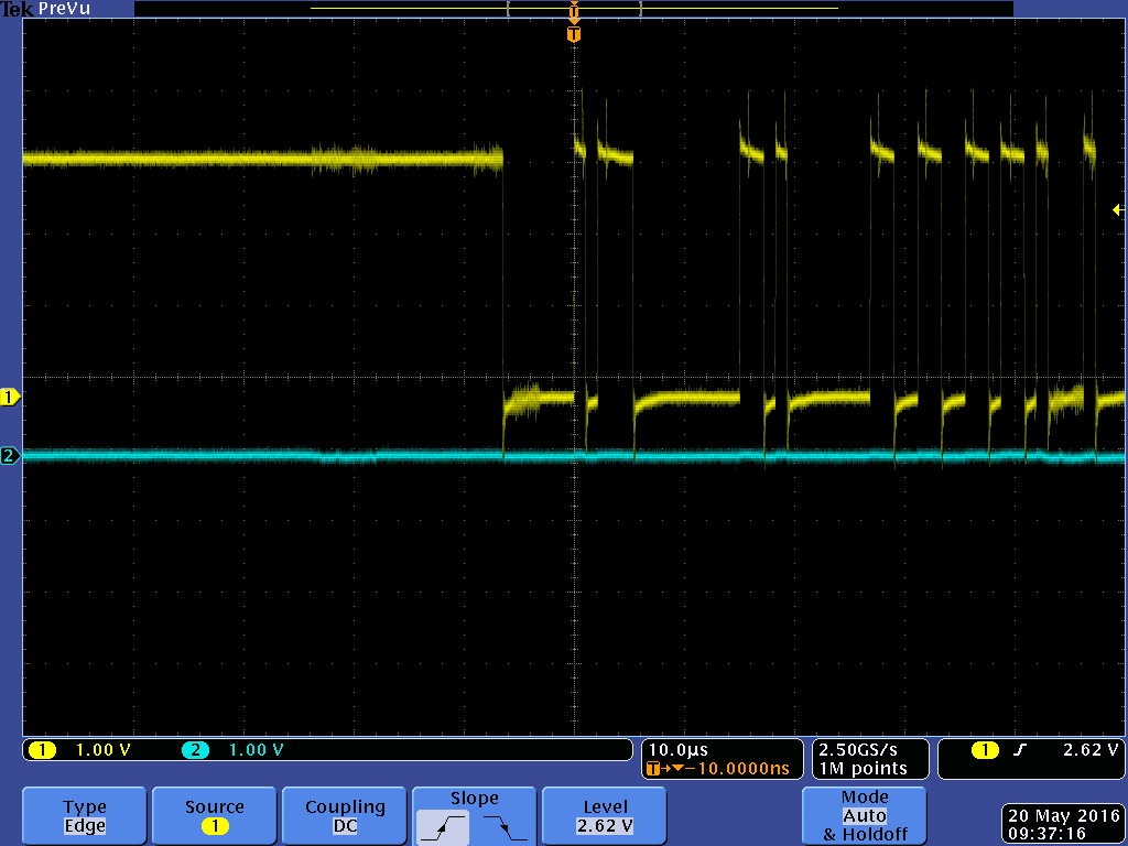
  • HI, Michael we have 120 ohm resistor between pin 6 and 7,( A & B). Right now the DE pin is tied to VCC of the transceiver and RE is tied to ground. Here is a pic of  pin 1(Channel 2 blue signal R) and pin 4( Channel 1 yellow signal D). I'm not using the TMs570 in LIN mode. The data sheet says we can run it with RE tied to ground so we can see the data on the R pin that we are sending on the D pin. Section 9.1 page 16

  • Hi Infane,

    I went a head in my lab and hooked up a SN65HVD1781 on the bench and captured a few scope shots for you. The device is configured with DE pulled to Vcc, /RE pulled to ground, and I am using a 10kHz square wave as my signal.

    The first image shows the input signal on the driver on channel 1, the output signal on the receiver on channel 2, and the bus signals on channels 3 and 4. The second image shows a measure of the propagation delay through the SN65HVD1781 from driver to receiver when they are both enabled simultaneously.

    Things you can check:

    1. Is /RE really pulled low? Is the receiver enabled?

    2. How is the GPIO pin on the TMS570 connected to the receiver output of the SN65HVD1781 configured? Is it pulled internally pulled low or high? Or is it configured as a input?

  •  Hi Micheal,

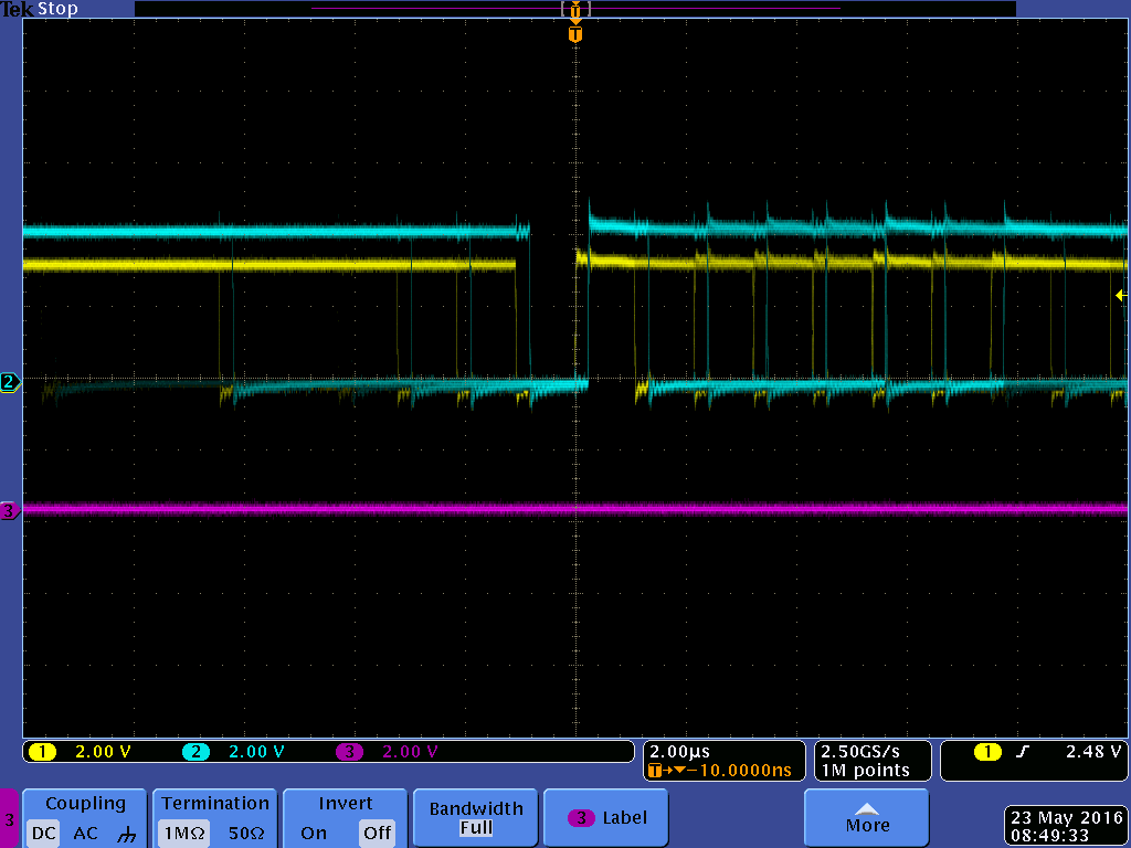
    Thanks for this information. We got it working. Channel 1 is the TX line and Channel 2 is the RX line.

  • Hi Infane,


    Glad to hear that you got it working! What ended up being the problem?