This thread has been locked.

If you have a related question, please click the "Ask a related question" button in the top right corner. The newly created question will be automatically linked to this question.

Enable signals of DS90CR287

Other Parts Discussed in Thread: DS90CR287

Hello,

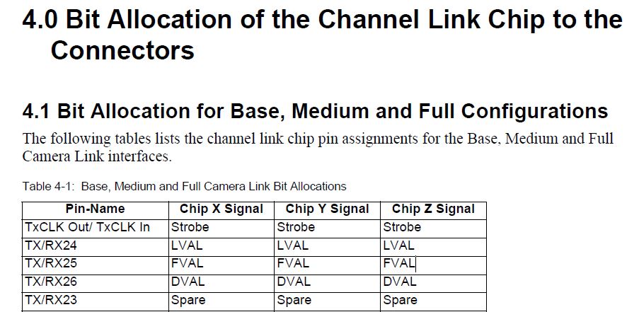
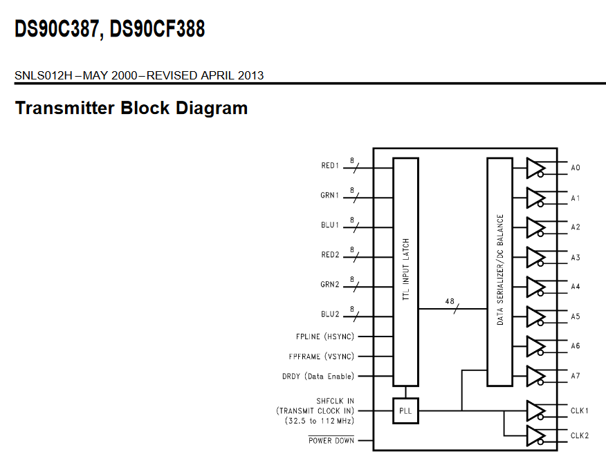
I'm confused about the enable signals(FVAL/LVAL/DVAL) of DS90CR287. I want use two DS90CR287 to implement a camera link medium interface, but I don't know if I can(or MUST?) connect the two enables signals to one source, and connect the two strb to one source, likes below:

thanks very much!

  • Hi,

    I'd like to understand the application a little better. Are you looking to send an identical camera output to two different displays? If so, it makes sense to use the same source for these signals to ensure that the display is identical. One note of caution I would add is that you must determine whether the driver for the input clock and enable signals (HSYNC, VSYNC, and DE) are capable of driving out to two pins, as there will be double the loading. Usually, I would expect to see a fan-out buffer used for this purpose.

    Regards,

    Michael
  • Hi,Michael


    Thanks very much for your reply. I am going to implement the "Camera Link" interface but not a general channel link. Data is transmitted from a camera to a frame grabber via camera link. The Camera Link Medium configuration needs two channel link chip, but I don't know how to connect the FVAL/LVAL/DVAL/Spare/CLK signals which defined in "Camera Link Specification 2.0".

     The standard say nothing, so I am not sure about it.

  • Hi,

    To connect these three signals, use the Bit Allocation specified in Section 4.1:

    FVAL (Frame Valid) = VSYNC

    LVAL (Line Valid) = HSYNC

    DVAL = DE

    Spare = Spare

    You will be able to compare that with the way that we typically see these signals connected to the DS90CR287, as shown in the following application note (see p. 6 for the matching Tx input signals):

    http://www.ti.com/lit/an/snla014/snla014.pdf

    Thanks,

    Michael

  • Hi, Michael

    Many thanks for your patience! So, refer to the DS90CR387's block diagram and the mapping table on p.6, I think I should connect two DS90CR287's FVAL/LVAL/DVAL/CLK to one source which generated by FPGA. Is that right?