


Hi,
I am using SN65DSI83 with OMAP 5432 ES2 to transform MIPI DSI to LVDS.
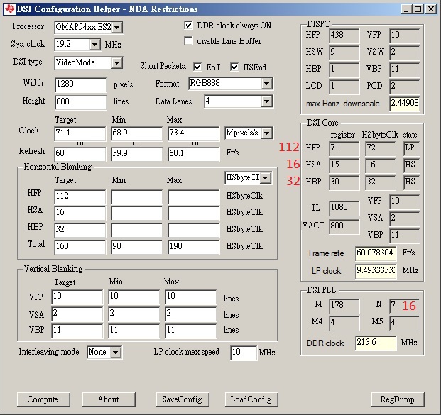
Currently, I could see the normal output screen or show the test pattern. (System Clock 19.2MHz, MIPI DSI clock 213MHz, LVDS clock 71 MHz)
However, in most of the time, IRQ register (0xE5) will show 0x81 (CHA_SYNCH_ERR, PLL_UNLOCK) in boot up.
Occasionally, IRQ register (0xE5) will show 0xB1 or 0x01.
Besides, it will show black or white screen in boot up state. (LVDS clock is enabled, and LVDS date pins output nothing.)
I would like to ask:
1. Why is the CHA_SYNCH_ERR bit is set in 0xE5 ?
2. How to solve the CHA_SYNCH_ERR ?
3. Is it normal to show PLL_UNLOCK ?
static struct omap_dss_device omap5_XXX_dsi_device = {
	.name                         = "lcd",
	.driver_name            = "sn65dsi83_i2c_d2l",
	.type                           = OMAP_DISPLAY_TYPE_DSI,
	.channel = OMAP_DSS_CHANNEL_LCD,
	.data	= &XXX_dsi_panel,
	.phy.dsi                = {
		.clk_lane       = 1,
		.clk_pol        = 0,
		.data1_lane     = 2,
		.data1_pol      = 0,
		.data2_lane     = 3,
		.data2_pol      = 0,
		.data3_lane     = 4,
		.data3_pol      = 0,
		.data4_lane     = 5,
		.data4_pol      = 0,
		.module         = 0,
		.ext_te = false,
		.ext_te_gpio = -1,
	},

	.clocks = {
		.dispc = {
			 .channel = {
				.lck_div        = 1,
				.pck_div        = 2,
				.lcd_clk_src    = OMAP_DSS_CLK_SRC_DSI_PLL_HSDIV_DISPC,
			},
			.dispc_fclk_src = OMAP_DSS_CLK_SRC_DSI_PLL_HSDIV_DISPC,
		},
		.dsi = {
			.regn                   = 16,
			.regm                 = 178,
			.regm_dispc     = 4,
			.regm_dsi       = 4,
			.lp_clk_div     = 18,
			.offset_ddr_clk = 0,
			.dsi_fclk_src   = OMAP_DSS_CLK_SRC_DSI_PLL_HSDIV_DSI,
		},
	},

	.panel = {
		.width_in_um = 216960,
		.height_in_um = 135600,
		.fb_xres = 1280,
		.fb_yres = 800,
		.dsi_mode = OMAP_DSS_DSI_VIDEO_MODE,
		.dsi_pix_fmt = OMAP_DSS_DSI_FMT_RGB888,
	},
	.reset_gpio     = SN65DSI83_EN,
	.max_backlight_level = 255,
	.set_backlight		= omap5XXX_set_bl_intensity,
};
static struct omap_video_timings sn65dsi83_timings = {
	.x_res		= 1280,
	.y_res		= 800,
	.pixel_clock	= 71100,

	.hsw			= 16,
	.hfp			= 112,
	.hbp			= 32,

	.vsw			= 2,
	.vfp			= 11,
	.vbp			= 10,
};

static const struct omap_dss_dsi_videomode_data vm_data = {
	.hsa			= 16,
	.hfp			= 112,
	.hbp			= 32,

	.vsa			= 2,
	.vfp			= 11,
	.vbp			= 10,

	.vp_de_pol		= true,
	.vp_vsync_pol		= true,
	.vp_hsync_pol		= true,
	.vp_hsync_end		= true,
	.vp_vsync_end		= true,

	.blanking_mode		= 1,
	.hsa_blanking_mode	= 1,
	.hfp_blanking_mode	= 1,
	.hbp_blanking_mode	= 1,

	.ddr_clk_always_on	= true,

	.window_sync		= 4,
};
unsigned char SN65DSI83_REGS[][2] =
{
	// Register Index, Set Value

	// Reset and Clock Registers
	{0x09, 0x00}, // SOFT_RESET
	{0x0A, 0x05}, // PLL_EN_STAT, LVDS_CLK_RANGE, HS_CLK_SRC
	{0x0B, 0x10}, // DSI_CLK_DIVIDER, REFCLK_MULTIPLIER
	{0x0D, 0x00}, // PLL_EN

	// DSI Registers
	{0x10, 0x26}, // LEFT_RIGHT_PIXELS, DSI_CHANNEL_MODE, CHA_DSI_LANES, SOT_ERR_TOL_DIS
	{0x11, 0x00}, // CHA_DSI_DATA_EQ, CHA_DSI_CLK_EQ
	{0x12, 0x2a}, // CHA_DSI_CLK_RANGE

	// LVDS Registers
	{0x18, 0x78}, // DE_NEG_POLARITY, HS_NEG_POLARITY, VS_NEG_POLARITY, LVDS_LINK_CFG, CHA_24BPP_MODE, CHA_2424BPP_FORMAT1
	{0x19, 0x00}, // CHA_LVDS_VOCM, CHA_LVDS_VOD_SWING
	{0x1A, 0x23}, // EVEN_ODD_SWAP, CHA_REVERSE_LVDS, CHA_LVDS_TERM
	{0x1B, 0x00}, // CHA_LVDS_CM_ADJUST

	// Video Registers
	{0x20, 0x00}, // CHA_ACTIVE_LINE_LINGTH_LOW     0x0500 (1280)
	{0x21, 0x05}, // CHA_ACTIVE_LINE_LINGTH_HIGH

	{0x24, 0x20}, // CHA_VERTICAL_DISPLAY_SIZE_LOW  0x0320 ( 800) [TEST PATTERN GENERATION PURPOSE ONLY]
	{0x25, 0x03}, // CHA_VERTICAL_DISPLAY_SIZE_HIGH               [TEST PATTERN GENERATION PURPOSE ONLY]

	{0x28, 0x21}, // CHA_SYNC_DELAY_LOW             0x0021 (  33)
	{0x29, 0x00}, // CHA_SYNC_DELAY_HIGH

	{0x2C, 0x10}, // CHA_HSYNC_PULSE_WIDTH_LOW      0x0010 (  16)
	{0x2D, 0x00}, // CHA_HSYNC_PULSE_WIDTH_HIGH

	{0x30, 0x02}, // CHA_VSYNC_PULSE_WIDTH_LOW      0x0002 (   2)
	{0x31, 0x00}, // CHA_VSYNC_PULSE_WIDTH_HIGH

	{0x34, 0x20}, // CHA_HORIZONTAL_BACK_PORCH      0x20   (  32)
	{0x36, 0x0b}, // CHA_VIRTICAL_BACK_PORCH        0x0b   (  11) [TEST PATTERN GENERATION PURPOSE ONLY]

	{0x38, 0x70}, // CHA_HORIZONTAL_FRONT_PORCH     0x70   ( 112) [TEST PATTERN GENERATION PURPOSE ONLY]
	{0x3A, 0x0a}, // CHA_VIRTICAL_FRONT_PORCH       0x0a   (  10) [TEST PATTERN GENERATION PURPOSE ONLY]

	{0x3C, 0x00}, // CHA_TEST_PATTERN                             [TEST PATTERN GENERATION PURPOSE ONLY]

	// IRQ Registers
	{0xE1, 0xFD},
	{0xE5, 0xFD},
	{0xE0, 0x01},
};

