This thread has been locked.

If you have a related question, please click the "Ask a related question" button in the top right corner. The newly created question will be automatically linked to this question.

TPL0102 Schematic Verification

Other Parts Discussed in Thread: LMV614

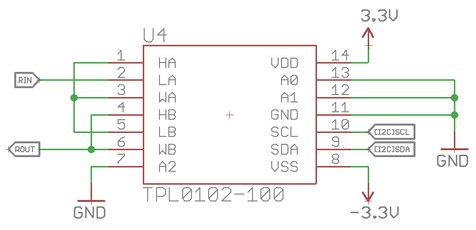
Hello, using the TPL0102 i'm aiming to use the device in rheostat mode as a variable resistor. Specifically, as mentioned in Section 7.1, Page. 11 of the datasheet to combine both channels to achieve 512 settings between 0 Ohms and 200kOhms.

  • I first wanted to verify that this was what is implied by that last paragraph where channel A is programmable between 0 - 100kOhms and B has the same capability and this is achieved by wiring the two channels in series?
  • In Section 7.4.3, Page. 14, the datasheet mentions that in Rheostat mode, the W and H terminals can be tied together. Is this also true when both channels are combined as shown in my schematic below? Should I just leave the HA and HB floating?

My schematic is attached below and I would appreciate it if anyone could verify that it is wired correctly. As mentioned above, my intentions are that between Rin and Rout there is a programmable resistance between 0 and 200kOhms.

  • Hello DMor,

    Thanks for the question.

    Generally, it is a good idea to short high and wiper together in rheostat mode (the idea is that if the wiper comes disconnected for some reason, you won't have a sudden disconnection in the current flow path). This applies more to a traditional potentiometer, rather than a solid state one, but is still ok to do.

    There is one issue, though. You are using a dual supply (+/- 3.3V), which techically violates the datasheet's limit for dual supply. You can do single supply 2.7 to 5.5V or dual supply 2.25 to 2.75 V.

    +/- 3.3V will likely cause long term damage to the device.

    If you can evaluate what the max and minimum voltages will occur on the Rout and Rin pins, you will need to verify that they fall within a range of Vss to Vdd.
  • That was a great catch with the voltage limit, I appreciate it. My updated schematic is attached below. The only thing I worry about is negative noise going into the RGAIN node in the order of -120 mV. The datasheet specifies it can handle -300mV, but that is also the absolute maximum ratings. Do you have any recommendations to ensure staying within the limits of the IC?

  • The -300 mV limit comes from the ESD diodes. At -0.3V, the ESD diodes will activate and you will begin drawing current from ground. If the diode current exceeds IIK (diode clamp current max), then damage to the diode is possible.

    -120 mV should not activate the diodes, but may cause some accuracy problems due to the way the internal switches are connected in silicon.

    Are you concerned with device damage for brief -120 mV transients? Or are you wanting to operate the device with -120 mV (relative to GND) on the RGAIN pin.

    Based on your schematic, looks like you're using it as a feedback path for an inverting op-amp setup. So it looks very much like you are expecting a positive and negative signal swing. Is it possible to get a +/- 2.5V supply setup for the TPL device?
  • This stage is occurring after a rectification stage using the LMV614, so it should only be minor spikes and not fully operating in this region. On the left should be an AC signal and on the output should be a positive and smoothed DC signal between 0 and 3.3v. I probed the node after R11 and it occasionally dips to around -120mV, although i'm not sure sure if its a measurement error on the oscilloscope or noise from the breadboard. Lowering the voltage to +/- 2.5v probably won't be an option.

  • DMor,

    Thanks. If it's only occasioinally dips to -120 mV, you should be fine. We recommend 0V as the lower limit simply because there is an ESD diode, but -120 mV should not cause any functional issues or reliability issues.