This thread has been locked.

If you have a related question, please click the "Ask a related question" button in the top right corner. The newly created question will be automatically linked to this question.

[TLK10232] macro for channel change

Hi team,

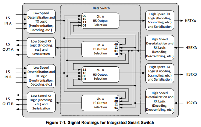
My customer want to connect ChB LS port to ChA HS port by only register settings. Could you tell me the macro for the channel change?

I'm guessing as below, but I'm not sure. Could you correct me if it's not enough?

//Setting for DATA Switch TX (LS=>HS direction)
To Ch-A phy address; 
Write a 0 to 0x1E.0017 bit 14
Write 2’b10 to 0x1E.0018 bits 15:14 

//Setting for DATA Switch RX (HS=>LS direction)
To Ch-A phy address; 
Write a 0 to 0x1E.0019 bit 14
Write 2’b11 to 0x1E.001A bits 15:14

Regards,

Takashi Onawa

  • Hi Takashi-san,

    To select an alternate channel LS input:

    CHANNEL A (LSB==>HSA direction):
    -Write 0x2800 to 0x1E.0017 (Applicable when the top level pin PRTAD0 is assigned to control transmit data-switch source input and if PRTAD0 is HIGH)

    -Write 0x2200 to 0x1E.0017 (Applicable when the top level pin PRTAD0 is assigned to control transmit data-switch source input and if PRTAD0 is LOW)


    When DST_PIN_SW_EN is LOW:

    -Write 0x8C20 to 0x1E.0018

    Regarding the RX direction, could you clarify the data-path? I mean, HSA ==> LSB?

    Best Regards,
    Luis Omar Moran
    High Speed Interface
    SWAT Team

  • Luis-san,

    Thank you for your quick reply.

    >Regarding the RX direction, could you clarify the data-path? I mean, HSA ==> LSB?

    Sorry, I should have explained more detail of their use case. please find the figure below.
    I just draw their use case.They want to switch Low side from Ch.A to Ch.B using same high speed lane like Ch.A. And they don't want to use PRTAD0 pin function.

    Regards,
    Takashi Onawa

  • Hi Takashi-san,


    For LSA <==> HSA (Set these values at Channel A)
    Write 0x2000 to 0x1E.0017
    Write 0x0C20 to 0x1E.0019
    00 = Select same channel LS input (default)

    For HSA <==> LSB (Set these values at Channel B)
    Write 0x2000 to 0x1E.0017
    Write 0xCC20 to 0x1E.0019
    11 = Select same channel LS input (default)

    Best Regards,
    Luis
  • Luis-san,

    Let me confirm your macro. It doesn't make sense for me. I might not understand this device behavior correctly... so Could you correct my understanding?

    In my understanding,  DST_CONTROL_2 register(0x0018) controls "HS Output Selection" Mux  and DSR_CONTROL_2 register(0x001A) controls "LS Output Selection" Mux  by only MIDO when PRTAD0 is NOT used.

    To connect LS OUT B to HSTXA and LS IN B to HSRXA, I thought "Ch.A HS Output Selection" and "Ch.B LS Output Selection" Mux's settings should be changed. So I thought   

    //Setting for DATA Switch TX (LS=>HS direction)
    To Ch-A phy address; 
    Write 1'b0 to 0x1E.0017 bit 14 (DST_PIN_SW_EN)
    Write 2’b10 to 0x1E.0018 bits 15:14 (DST_DATA_SRC_SEL[1:0])

    //Setting for DATA Switch RX (HS=>LS direction)
    To Ch-A Ch-B phy address; 
    Write 1'b to 0x1E.0019 bit 14 (DSR_PIN_SW_EN)
    Write 2’b11 to 0x1E.001A bits 15:14 (DSR_DATA_SRC_SEL[1:0])

    Regards,

    Takashi Onawa

  • Hi Takashi-san,

    Sorry for my mistake. The configuration is as follows:

    //Setting for DATA Switch TX (LSB=>HSA direction)
    To Ch-A phy address;
    Write 1'b0 to 0x1E.0017 bit 12 (DST_PIN_SW_EN)
    Write 2’b10 to 0x1E.0018 bits 15:14 (DST_DATA_SRC_SEL[1:0]) //Selects data from Low Speed CHB to High Speed CHA

    //Setting for DATA Switch RX (HS=>LS direction)
    To Ch-A Ch-B phy address;
    Write 1'b to 0x1E.0019 bit 12 (DSR_PIN_SW_EN)
    Write 2’b11 to 0x1E.001A bits 15:14 (DSR_DATA_SRC_SEL[1:0])

    Best Regards,
    Luis
  • Luis-san,

    Thanks. I could understand the switching behavior of this device completely.

    Regards,
    Takshi Onawa
  • Great! Please let me know if you have further questions on this device.

    Regards,

    Luis