This thread has been locked.

If you have a related question, please click the "Ask a related question" button in the top right corner. The newly created question will be automatically linked to this question.

PCA9306: Level shift

Part Number: PCA9306

Hello team,

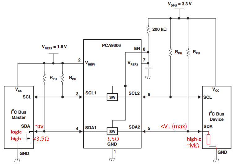
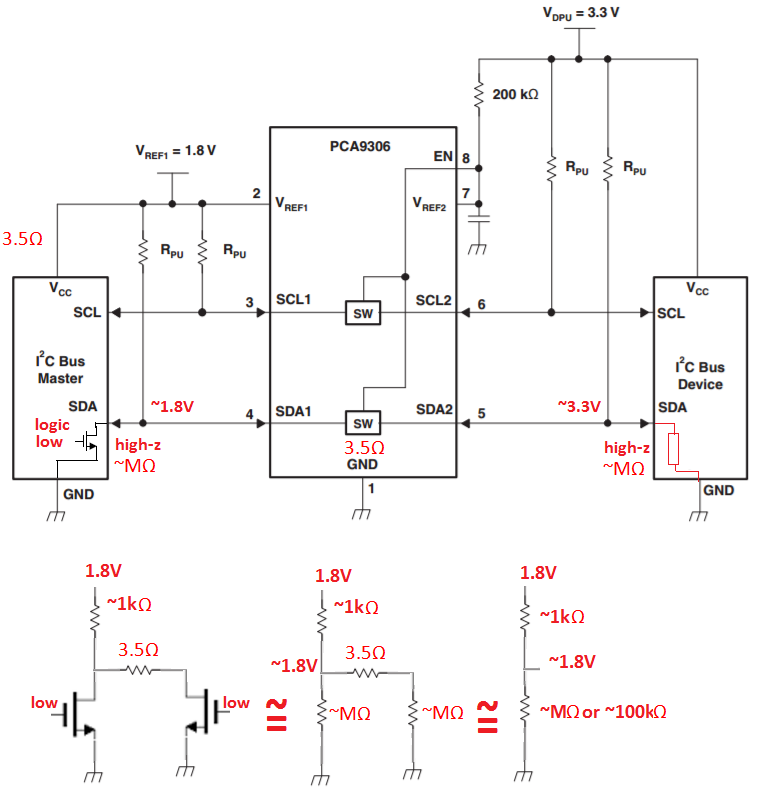
Below is PCA9306 typical application, switch is always enabled.If the signal transfer from 1.8V side to 3.3V side, when there is 1.8V high level input signal, you know the Ron of our part is about 3.5ohm, so there is 3.5ohm+ Rpu resistor between 1.8V and 3.3V, because the Ron of our part is very small, so the voltage of output of 3.3V side should be very close to 1.8V level, so how does the output transfer to 3.3V level?

1. For this application, the switch should be always enabled, and the Ron is about 3.5ohm all the time, correct?

Regards,

nanfang

  • Hello Nanfang,

    I think you may be overlooking part of the circuit. On the SDA and SCL lines of the I2C slave or master bus is a mosfet that leads to ground (open drain configuration seen in figure below). This internal FET forms a voltage divider with the pull-up resistor. When the FET gate is low and the FET is off, the voltage on the data or clock is essentially the supply voltage. The ron provides a path between the two different biases.

  • Hello Patrick,

    Thanks, so you mean switch is on when there is low level signal, and when there is high level signal, the switch should be off, correct? Can you give me detail description which pin connects to Vcc, which pin connects to SDA/SCL pin of the circuit you provided above?

    Regards,

    Nanfang

  • Hello Nanfang,
    The diagram you attached on your first post shows how the PCA9306 is connected for your application.
    -Francis Houde
  • Hello Nanfang,

    The image below gives an example of how a low bit is passed from the I2C bus master to another I2C bus device.  Essentially when a low bit is desired, the internal FET's gate is given a logic high signal, which pulls the node connecting the SDA and pull-up low.  It will not be zero as the internal FET also has a Ron value, but I will be close to 0V.  When the PCA9306 is enabled, this will also pull the SDA2 node low.  The SDA2 node will not be 0V, but it will be low enough to satisfy the VIL (low level input voltage) requirement of the receiving I2C bus device.

  • Hello Patrick,

    Thanks you very much, i kow how low bit pass from one side to another side, but can you also explain how does high bit pass?

    Regards,
    Nanfang
  • Hello Nanfang,

    The images below should illustrate the concept.  If you utilize the principle of superposition and simplify the circuit, you can see that the internal mosfets with the pull-up resistor form a voltage divider.  As the FETs have a large resistance (100x or so greater than the pull-up), very little voltage will be dropped across the pull-up.  Thus the pin to I2C bus should have a voltage very close to the supply voltage.  The internal resistance (Ron) of an enabled PCA9306 provides a bridge between the two supplies.