This thread has been locked.

If you have a related question, please click the "Ask a related question" button in the top right corner. The newly created question will be automatically linked to this question.

PCA9515A: I2C communication issue

Part Number: PCA9515A
Other Parts Discussed in Thread: PCA9515,

Hello everybody,

Please apologize my bad english and my lack of digital skills as I'm basically an analog guy !!!

I'm having monitoring issues on an I2C bus with a PCA9515 used as a switch/buffer on the I2C entry of my daughter board (mother board I2C is not affected anyway)

If I bypass the PCA everything is working perfectly. When PCA9515A is populated, it seems that control is working (I2C Master -> slaves) but I'm having a buggy monitoring on I2C peripherals.

In it's simplest configuration, my daughter board includes only 2 I2C slaves: temp sensor MAX7500 & a demodulator STV0910 from ST.

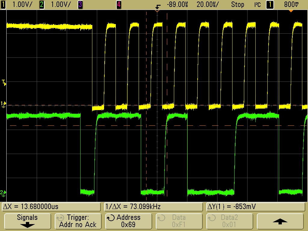
Here is an scope plot when all is OK (no PCA9515):

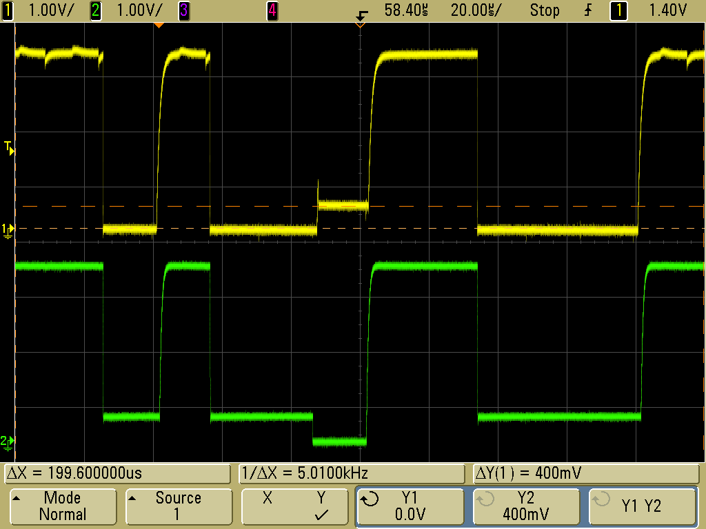
An here when PCA9515 is on the line:

I know that the 0.5V offsets are inserted by the PCA9515 to insure stability between read & write sessions on the bus but my guess is that these 0 logic level offsets could disturb the chips on the bus.

Does anybody have experienced the same troubles ?

And most important: is there a solution ?

Thank you for your help.

Yann

  • Hello Yan,
    Can you show me your schematic? I want to see how you have connected the devices and what values you have for components.
    -Francis Houde
  • Hello Francis,

    Glad to read from you. Here are the I2C elements from my schematic:

    As you can see U2 (PCA9515A) in the input I2C device of my board. Now I'm running the board with U2 removed and R40+R43 mounted (PCA bypass) and it works.

    On the 2 other pics you can see we use only 2 I2C chips. When PCA9515 is online, I'm having trouble with U10 monitioring: the GUI indicates bad or frozen values but I know it's working normaly. That's what makes me thinking that U10 is correctly controlled an programmed but readings are affected.

    Thanks for your help.

    Yann

  • Hello again Francis,
    I forgot to mention that we have also 2 10K pullup res. connected between SCK, SDA and P3V3 (they do not appear on the above partial schematics)
    Yann
  • Hello Yann,
    Sorry for the delay in response. This post fell through the cracks. That is my fault.

    I have several questions for you.

    1) I can't seem to find the STV09100 datasheet so I couldn't find Vol, Vil information and the test conditions they are tested at.

    2) Are you doing level translation from the motherboard to the daughter card? or are they at the same voltage of 3.3V?

    3) Is the Power Good, an active high or low?

    4) I am assuming that the net label DEMOD_SCK/SCL goes to L2 and L1 pins of U10A, can you confirm.

    5) Can you capture waveforms on both sides of the buffer during the transactions?

    6) I seem to be seeing an oscillation riding on the SDA/SCL lines. It that an artifact of how you are measuring the signal or is it real? Can you confirm that the supply isn't oscillating.

    7) what is driving the mother board side SCL/SDA lines and what pullups do they have?

    My main concern is that there is a mismatch on Vol/Vil and the static voltage offset of the part is not working properly.
    -Francis Houde
  • Hello Francis,

    It's good to read from you !

    Here are some answers to your questions:

    1) DC specifications of the digital IO's of the STV0910 chip:

    Vil: -0.3 to +0.8V

    Vih: 2.0 to 3.6V

    Vol: 0.4V max.

    Voh: 2.6V min.

    2) No level translation. Mother Board I2C is also at 3.3V.

    3) PGOOD is active high

    4) No. DEMOD_SCK & DEMOD_SDA are connected to U10A B14 & B13 pins. A11/B11 and L2/L1 are independent I2C auxiliary buses that are not connected to the main I2C we are talking about.

    5) Unfortunately not at this time. I have no board available immediately but I agree with you: it's an interesting measurement that I should have already made !

    6) Power supplies were checked. I think this oscillations come from my bad scope probes with a too long ground connection.

    7) Mother Board I2C is driven by a PowerQuick processor (MPC8378VRALGA) with 10K pullups tied to +3.3V

    Hope this can help.

    Once again thank you for your support.

    Yann

  • Hello Yann,
    Have you been able to capture all four waveforms when you have problems with the communications? I don't really see a problem with the waveforms you sent. The static voltage offset seems to be working fine, but I really need to see if the zero's are propagating across the device correctly, for both SCL and SDA.

    You might want to let me know what the current is for the given Vol of the STV0910. Are you able to communicate with other devices on the same node? Does the MAX7500 work ok?
    -Francis Houde
  • Hello Francis,

    Here are the captures on both sides of the PCA9515 :

    SCL:

    SDA:

    On each plot upper yellow curve is taken on the master/mother board side (SCL0/SDA0) and green curve is probed on the slave/daughter board side (SCL1/SDA1)

    The STV0910 output sink current (Iol) spec is 4mA max. To answer your last question,I can't tell you because the firmware guys have not included this chip in the overall board monitoring..... sorry.

    Yann.

  • Hello Francis,

    Any news ?

    Yann

  • Hello Yann,
    I am running out of ideas of what your problem might be if you can't show me the I2C transactions on both sides of the buffer at the time of the error.

    1) Have you verified that you are within the I2C specifications for rise times on both sides of the buffer?

    2) I did notice that you looks like you have close coupling on between the SCL and SDA and SDA seems to have noise coupling due to clock. Have you separated likes to see if that helps? I don't think that is the issue, but given that I don't have the physical board here to probe I just wanted to ask.

    3) Have you tried different pull up resistors on both sides of the buffer? Have you estimated capacitances on both sides of the buffer?

    I don't know what else I can do remotely to help unless you can repeatedly get the problem to occur and then show waveforms from both sides of the buffer during that incorrect I2C transaction.
    -Francis Houde
  • Hello Francis,

    It's been a long time ...

    At least I had the opportunity to work with a secondary and simplest slave peripheral: the temperature sensor MAX7500. I think I have made very interesting discoveries. Trying to monitor board temperature from my GUI interface I had permanent errors indicating negative temperatures (board is on the bench at room temp) This didn't occur when the PCA9515 was bypassed. Except this data value problem, I have no I2C read/write issue.

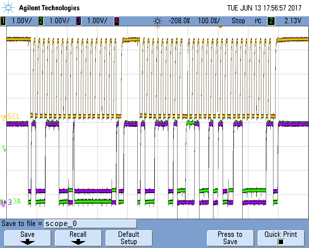
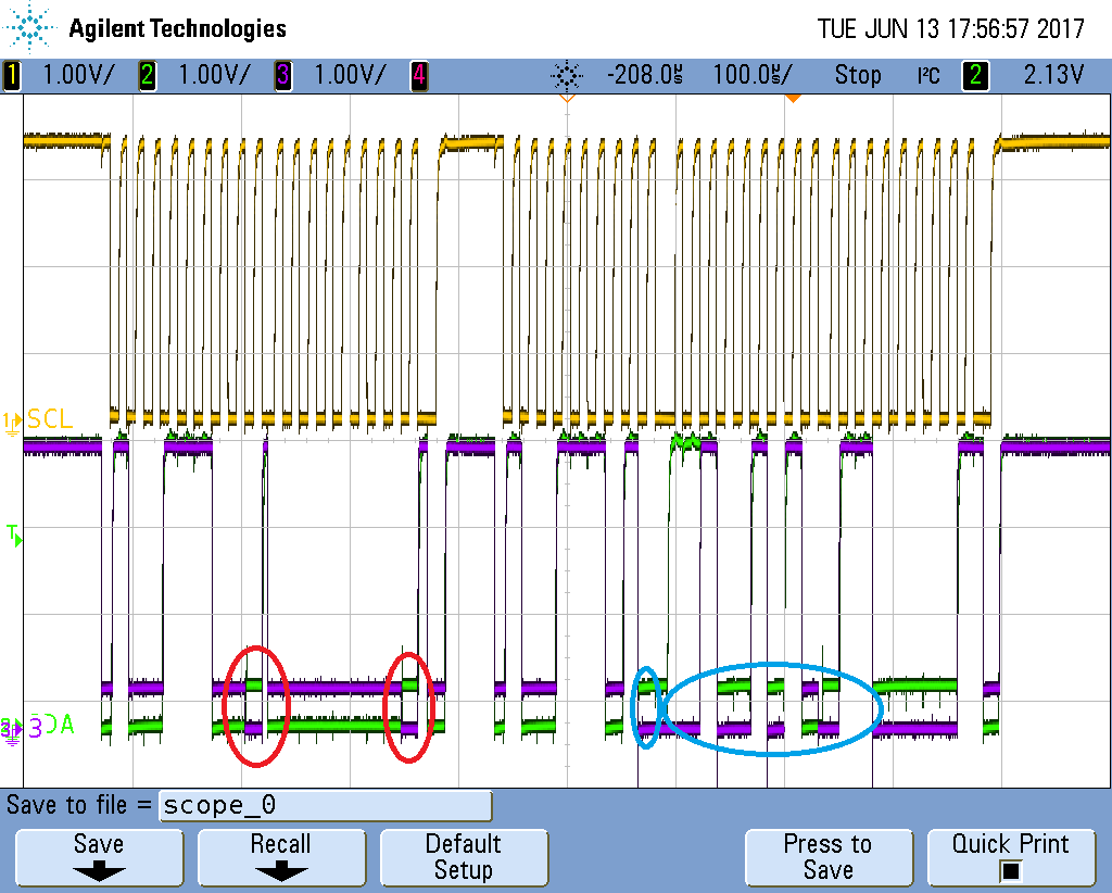
    You'll find hereafter 2 scope plots made around the PCA9515.

    Yellow trace is the SCL signal seen from the master side of the PCA (PCA9515-p2 SCL0)

    Green trace is the SDA signal seen from the master side of the PCA (PCA9515-p3 SDA0)

    Purple trace is the SDA signal seen from the slave side of the PCA (PCA9515-p6 SDA1)


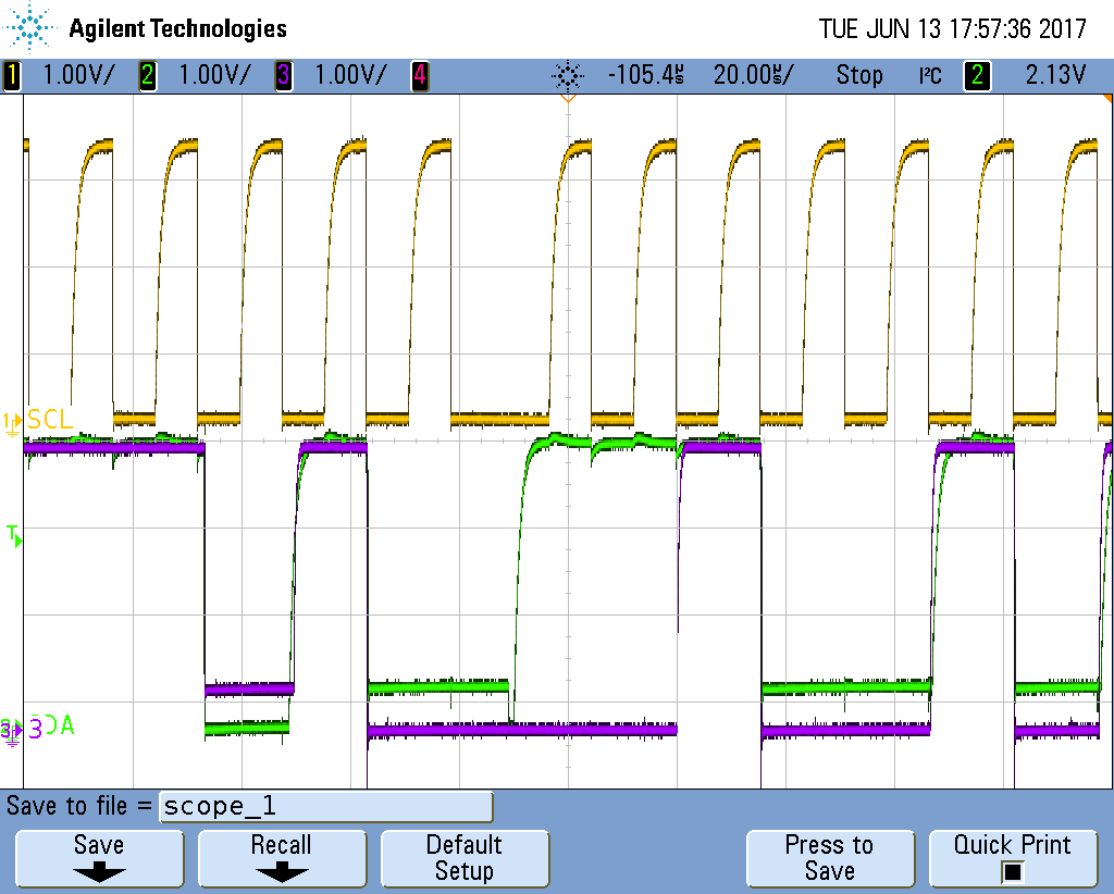
    As you can see above (1st plot) everything seems to be OK during start/stop/ACK and write sequences. But you can notice that during the read sequence there is a difference between the "SDA" in & "SDA out". Plot2 is a zoom of this critical period. We can see there that the 2 first bits sent by the probe (00 value) are inverted on the master side of the PCA. The first bit denotes the sign of the monitored temperature. This is a perfect explanation why I read altered temperature values.

    Of course the question is:  why these 2 bits have been change by the PCA? ?  If I had level or slew rate issues I would have random errors. But here the error occurs always at the same time . . . Strange behaviour isn'it ?

    Many thanks in advance for your help Francis.

    Yann

  • Yann,

    This is indeed peculiar, and you mentioned it happens at the same spot every time, do you mean at that point in the read frame every time? The interesting part is that it's happening on the 8th falling edge, at which point the master will let go of the data line and the PCA9515 will take over holding it to a logic low, this explains the master and slave logic lows "swapping" places in the logic low position. This is explained in section 9.1.2 of the datasheet with a bit more detail. In the image below I've circled in red where this is happening. Once the master has transmitted the 9th clock pulse, the slave releases the data line and the master takes back over. This is also shown in the pulses following the red circles.

    However, if you look at where the error occurs - at the blue circle -  the master doesn't seem to take back over after the 9th clock pulse, and the slave device is still the one holding the data line down, and this persists for the rest of the frame. I'm not sure if this is related to the error you're seeing, but it's definitely worth noting because this is not the correct behavior.

    Is there any chance you can capture the error with a different message frame, and get the clock from the slave side as well on the screenshot? This will show if this same behavior is seen at a different failure point, and if the SCL on the slave side behaves correctly while this error is happening. It almost looks like the slave side i missing some clock pulses then kicks back in after a few bits.

    Regards,

  • Hi Eric,

    Many thanks for your feedback.

    About your remarks in the blue circle area, have you noticed that we're entering into the read mode so the slave (temp sensor) is driving the SDA line during 8 clock cycles and ACK ? For us, this is a normal behaviour. Apparently you are thinking about a clock streching or "pause" requested by the slave by holding SCL to 0. But when looking at the SDA, data is available with no delay . . .

    To make sure there is no understanding error on this critical area, I will try to re-capture signals with both SCL sides as you suggested. Talk to you soon.

    Best regards.

    Yann

  • Hello Yann,

    One thing I am noticing is that during the clock stretching (see red square) the Master does something it isn't supposed to do, pull down on the bus (see red circle).  

    I also know that some of our older parts had some race conditions due to glitches on the bus.  Here is the errata that covers it.  I am wondering if this might be a similar problem that we haven't seen before.

    I would try and see if you can get the master to not glitch during the clock stretching event.

    -Francis Houde