This thread has been locked.

If you have a related question, please click the "Ask a related question" button in the top right corner. The newly created question will be automatically linked to this question.

SN65HVD09: Fail safe termination design and calculation

Part Number: SN65HVD09


Hi,

I am planning to use SN65HVD09 transceiver in my design for RS422 application for the operating speed of 10Mbps, I need some clarification related to the Fail safe design calculation at the Input of the chip if operating as Receiver.

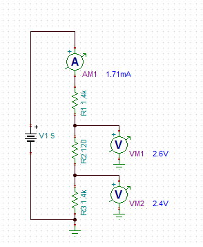
Fail safe resistors used are 1.4K ohm for both pull up and pull down and 120 ohm termination resistor at differential line. While in Stop condition 1B+ is assumed as High(Vcc=+5V) & 1B- is set to be Low(Ground).

1. What will be the current flowing through the Rc(120 Ohm) resistor when the Chip in not receiving any data?

2. How to Derate the power consumed by Termination resistor(Rc) and what power watts to be selected for resistor not to fail.

Regards,

M Lokesh

  • Hi M Lokesh,

    1. The input resistance of the bus pins on the SN65HVD09 is ~12k ohms per the TIA/EIA-485 specification so the leakage current flowing into the device will be at a minimal. Ifs or the current flowing through the failsafe resistor network (1.4k, 120, 1.4k) in a steady state condition will be ~1.7mA. Here is the circuit in the TI simulation tool:

    2. The failsafe resistors do not need to be sized for large amounts of power unless you are over compensating for transient protection where the instantaneous power can get very high (i.e. IEC ESD 61000-4-2 or IEC Surge IEC 61000-4-5). In a steady state condition the max power that should be seen with the parameters above is ~4mW (P = I^2/R).

    Please let me know what other questions you have and I will be glad to help!