This thread has been locked.

If you have a related question, please click the "Ask a related question" button in the top right corner. The newly created question will be automatically linked to this question.

PCF8574: Steps to Switch ON 8-relays connected in PCF8754

Part Number: PCF8574

Hello,

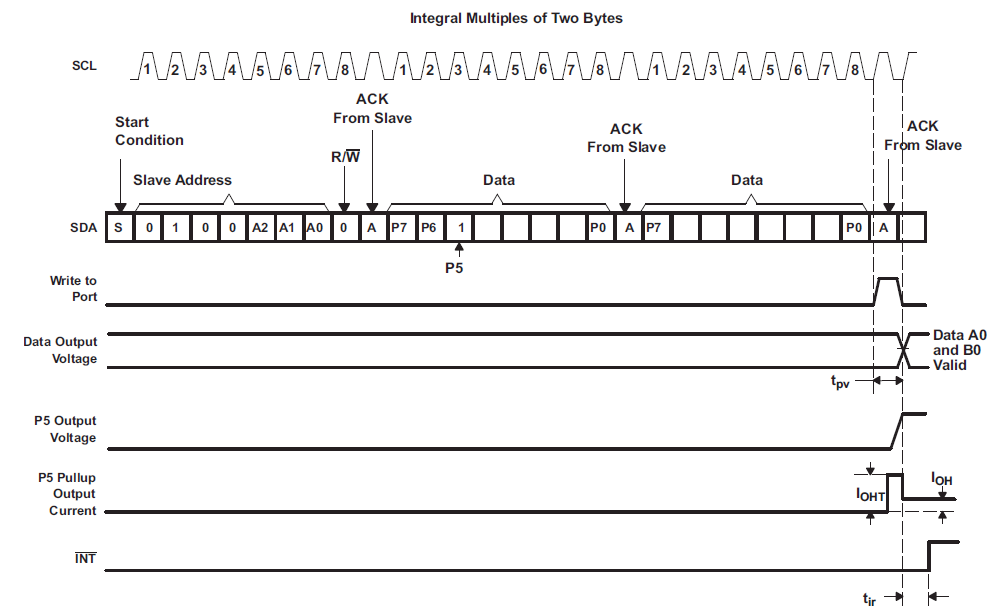
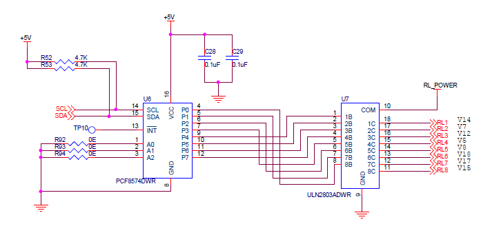
I am working a project where I am using PIC18F4620 MCU with PCF8574 to switch ON the 8 connected relays in their 8 Port pins. Coming to I2C communication, first I am sending start bit, then slave address and 0xFF to switch on all relays in the 8 port pins. Is this right way to deal with PCF8574?. Or  should I send any commands to configure PCF8574's port direction before sending output high (0xFF) at port pins. Can anyone guide me for I2C communication between PIC18F4620 and PCF8574 . My application need Port write mode only. I don't want Port read features from PCF8574. Below is the schematic that I used to interface PIC18F4620 MCU and PCF8574. Please suggest a solution.

Thanks,

Muthu

  • Hello Muthu,

    If you only want to do writes, then make sure you toggle the write bit at the end after the last address bit.  Keep in mind that it will have to cycle through the shift register. 

    -Francis Houde 

  • Hi Francis Houde,
    Thanks. I have some questions to ask regarding IO expander functions.

    Q1. After sending slave address, Should I send any Command byte to configure PCF8574 Port pin's direction (Input or Output) ?.

    Q2. I need to write logic high at all 8 port pins. What byte Should I send to make all 8 port pins logic high after addressing slave ?.

    Q3. In Our side, I am trying with 0xFF to make 8 Port pins logic high (5V). When I measured voltage at Port pins after writing this 0xFF, I am getting 0.8V instead 5V.


    Please suggest a solution.


    Thanks,
    Shankar
  • Hi Francis Houde,

    PCF8574 NXP part is working but the same part from TI is not working. I don't see any difference in specifications. I can see device's acknowldgement after sending Address and Data (0xFF) in TI's PCF8574 but it is not staying  at state which I wrote (0xFF).When I write 0xFF as data, P0-P7 staying in some milliseconds. After that, it goes to OFF state. Here is Our schematic

    Thanks,

    Muthu

  • Hello Muthu,

    Can you record the I2C transactions with a  scope so that I can see it?  I want to make sure the signals look ok and make sure that the format is correct.

    -Francis Houde

  • Hi Francis Houde,

    Attached Oscilloscope image. In this, for first 8 clocks, I am sending address 0x44(include write bit 0). Then, in the 9th clock, slave responds with low. For next  8 clocks, I am sending data 0x01. Then slave responds with 0.

    Thanks,

    Muhtu

  • Hi Francis Houde,

    Please find the attached image with remarks so that you can easily get in to further queries.

    Thanks,

    Muthu

  • Hi Francis Houde,

    Still I am waiting for your reply. We will purchase in volumes if TI-PCF8574 gets Ok. Other wise we have to move NXP. Hope, We will get soultion from TI.

    Thanks,

    Muthu

  • Hi Muthu,

    Sorry for the delay - Francis is out of the office right now, so I am taking a look at this for him.

    There are a couple things I wanted to point out based on the waveform captures you provided. I see on your schematic that you have all three address lines pulled low; if this is the case, then the device address that you should use for a "write" operation is 0x40. Also, the datasheet indicates that two bytes of data transfer are required for full device programming (see Figure 12 as well as the note on the figure that Francis referenced in his earlier post). I'd recommend adding another eight cycles of 0xFF data following the ACK in your waveforms; the P[7:0] outputs should then be valid following the third ACK.

    I hope this helps, and please let me know if you are still having trouble.

    Best regards,
    Max
  • Hi Max,

    Thanks. What do u mean by two byte programming ?. Right now, I am sending salve address followed by DATA (0xFF) to set Port pins as Output logic high. As per datasheet, this is two byte programming.

    Please let me know If I understood anything wrong in this.

    Thanks,

    Muthu

  • Hi Muthu,

    In the image Francis copied above, there are three 8-bit transactions. The first communicates a slave address and indicates whether the operation is a read or write. The second two each define the P[7:0] values. I realize this is a little strange given that there are only 8 port values to assign, but could you try sending the P[7:0] values twice after the address? The figure shows the configured values not actually being transferred from the internal shift register to the output ports until this second data byte (third byte total if you include the address) is written and acknowledged.

    Max
  • Hello,

    We have tried this, there is no difference.

    However now we have solved the problem by changing the device to PCF8574at/3.518, this is working absolutely to spec.

    not able to still figure out why TI is not working. By datasheet i dont see any difference.

    Regards,
    Muthu