Other Parts Discussed in Thread: DS90UB925Q-Q1, , DS90UH927Q-Q1, DS90UB928Q-Q1, DS90UH925Q-Q1
Hi Team,
The customer is using DS90UB925Q-Q1 and DS90UH928Q-Q1. The input signals is LVCMOS for the customer's application. So the customer
uses DS90UB925Q-Q1, not 927.
The block diagram is the input signals>>>DS90UB925Q-Q1>>>DS90UH928Q-Q1>>>LVDS
Display. The GPIO0 pin(25 pin) for 925 has the PWM waveform. The frequency of PWM is 1KHZ and the duty cycle is 50%.
The image is fine on the LVDS display screen. But the GPIO0 pin(14 pin) for 928 is always the low level. The low level voltage is about 0V.
The register configuration is as follows:
925:
0x03 = 0x9A
0x12 = 0x04
0x0d = 0xA3
928:
0x22 = 0x04
0x1d = 0x25
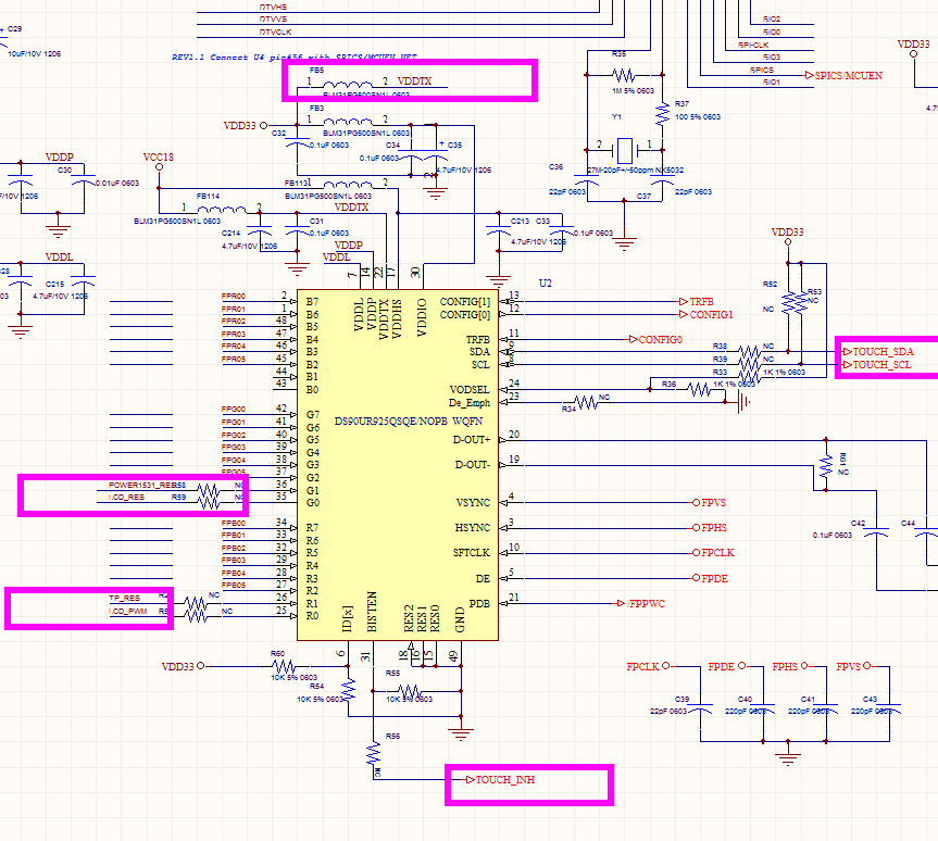
The schematic of 925 is in the attach. The customer cannot provide the schematic of 928 since another customer designs the schematic of 928.
Q1: Can DS90UB925Q-Q1 and DS90UH928Q-Q1 be used together at this case?
Q2: Can you check the register configuration and the schematic of 925?
Best Wishes,
Mickey Zhang
Asia Customer Support Center
Texas Instruments