Other Parts Discussed in Thread: TEST2
Hi,
We used the combination of DS90UB927(TX) and DS90UB928(RX) for LCD and KEY transmission.
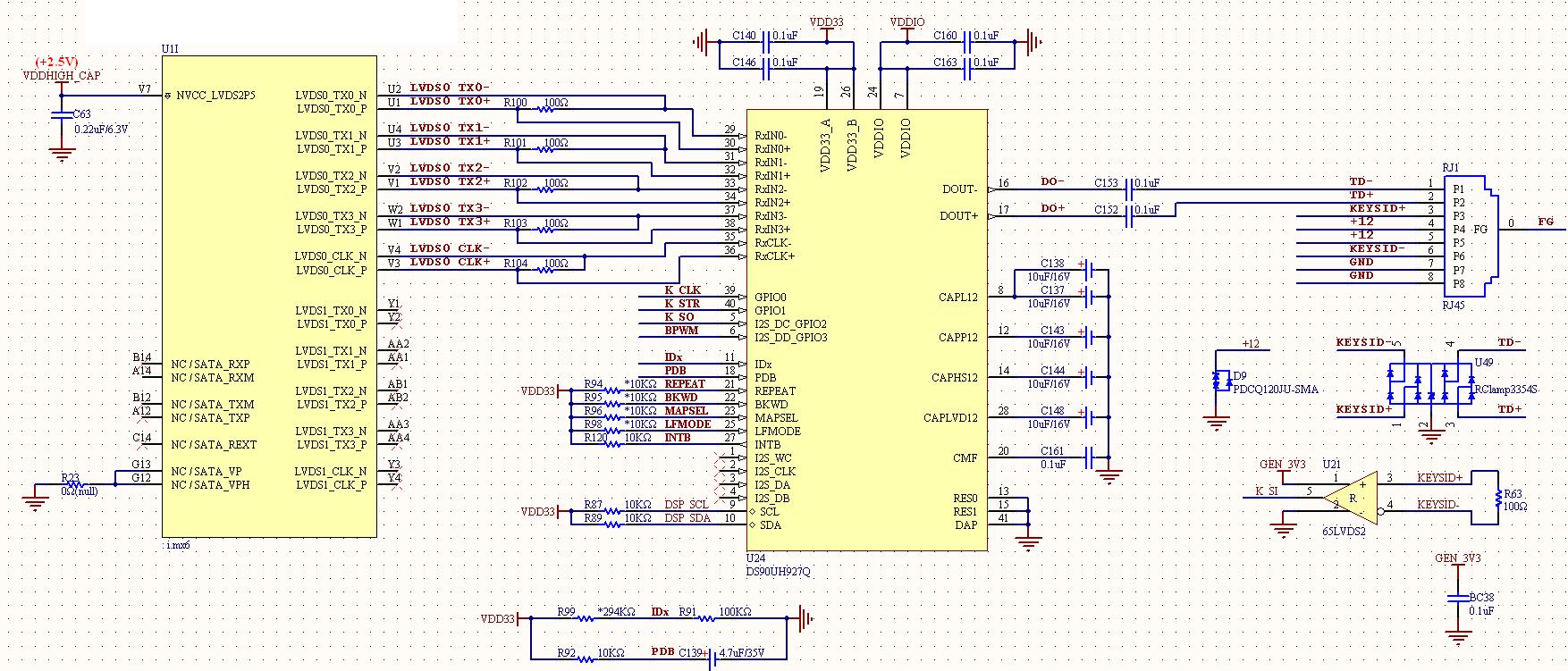
(a)The hardware configure of DS90UB927(TX).
Repeat=low
BKWD=low
MAPSEL=low
LFMODE=low
LVDS_CLK=65MHz
DS90UB927 schematic
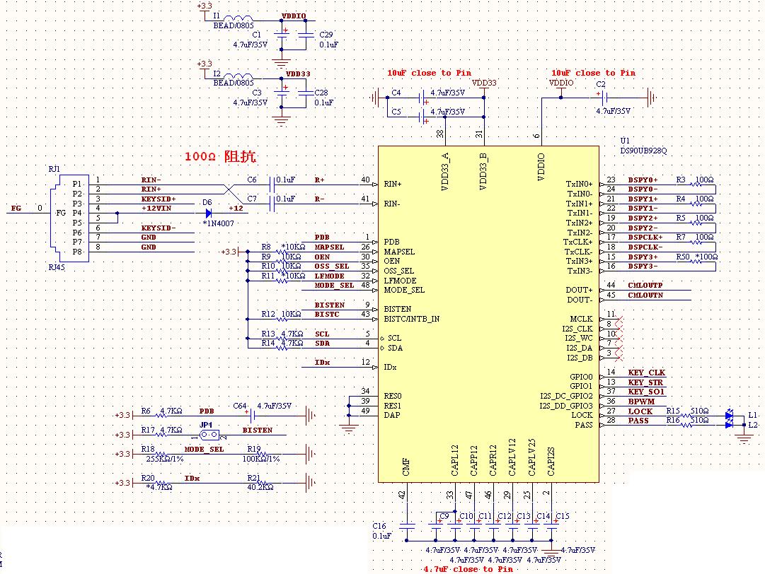
(b)The hardware configure of DS90UB928(RX).
MAPSEL=low
OEN=high
OSS_SEL=high
LFMODE=low
REPEAT=low
BKWD=low
I2S_B=low
LCBL=high
DS90UB928 schematic
Using GPIO[3:0] for KEY transmission. When power up, we enable 927 and 928 GPIO[3:0] with I2C.
(c)DS90UB927(TX) software config to enable GPIO
0x0D=0x03
0x0E=0x33
0x0f=0x03
(d)DS90UB928(RX) software config to enable GPIO
0x1D=0x05
0x0E=0x55
0x0f=0x05
TEST1: GPIO[3:0] of DS90UB927 input 800KHz, 400KHz, 200KHz, 10KHz continuous clock respectively. (40MHz clock source use frequency divider (CPLD) generates 800KHz, 400KHz, 200KHz, 10KHz)
Result: The LOCK and the PASS pin of DS90UB928 both output high, LCD displays normally, and GPIO[3:0] of DS90UB928 outputs 800KHz, 400KHz, 200KHz, 10KHz continuous clock respectively.
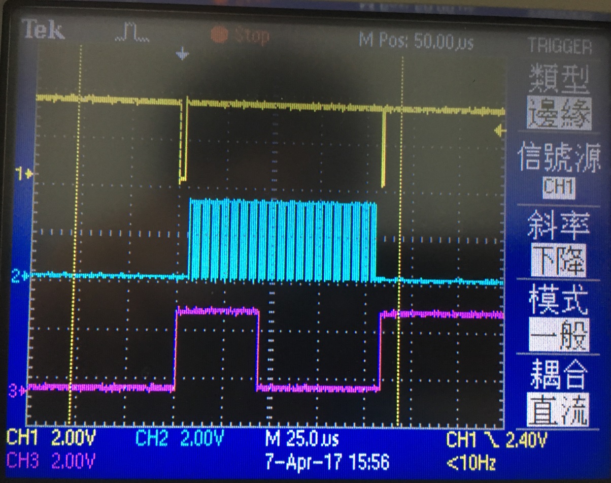
TEST2: Please refer to the waveform of the scope(shown as below), GPIO[2:0] of DS90UB927 input chanel[3:1] signal respectively. (these signals output from CPLD)
Result: The LOCK and the PASS pin of DS90UB928 both output low, LCD can't display(no signal), and GPIO[2:0] of DS90UB928 always output low.
TEST3: Please refer to the waveform of the scope(shown as below), GPIO[2:0] of DS90UB927 input chanel[1] signal.
Result: The LOCK and the PASS pin of DS90UB928 both output high, LCD displays normally, and GPIO[3:0] of DS90UB928 outputs chanel[1] signal.
TEST4: Please refer to the waveform of the scope(shown as below), GPIO[2:0] of DS90UB927 input chanel[2] signal. (400Khz)
Result: The LOCK and the PASS pin of DS90UB928 both output high, LCD displays normally, and GPIO[3:0] of DS90UB928 outputs chanel[2] signal.
Question: Why DS90UB928 can't lock under test2 condition?