This thread has been locked.

If you have a related question, please click the "Ask a related question" button in the top right corner. The newly created question will be automatically linked to this question.

SN65DPHY440SS: Are There Restrictions To Using Lane0 With a MIPI Camera?

Part Number: SN65DPHY440SS

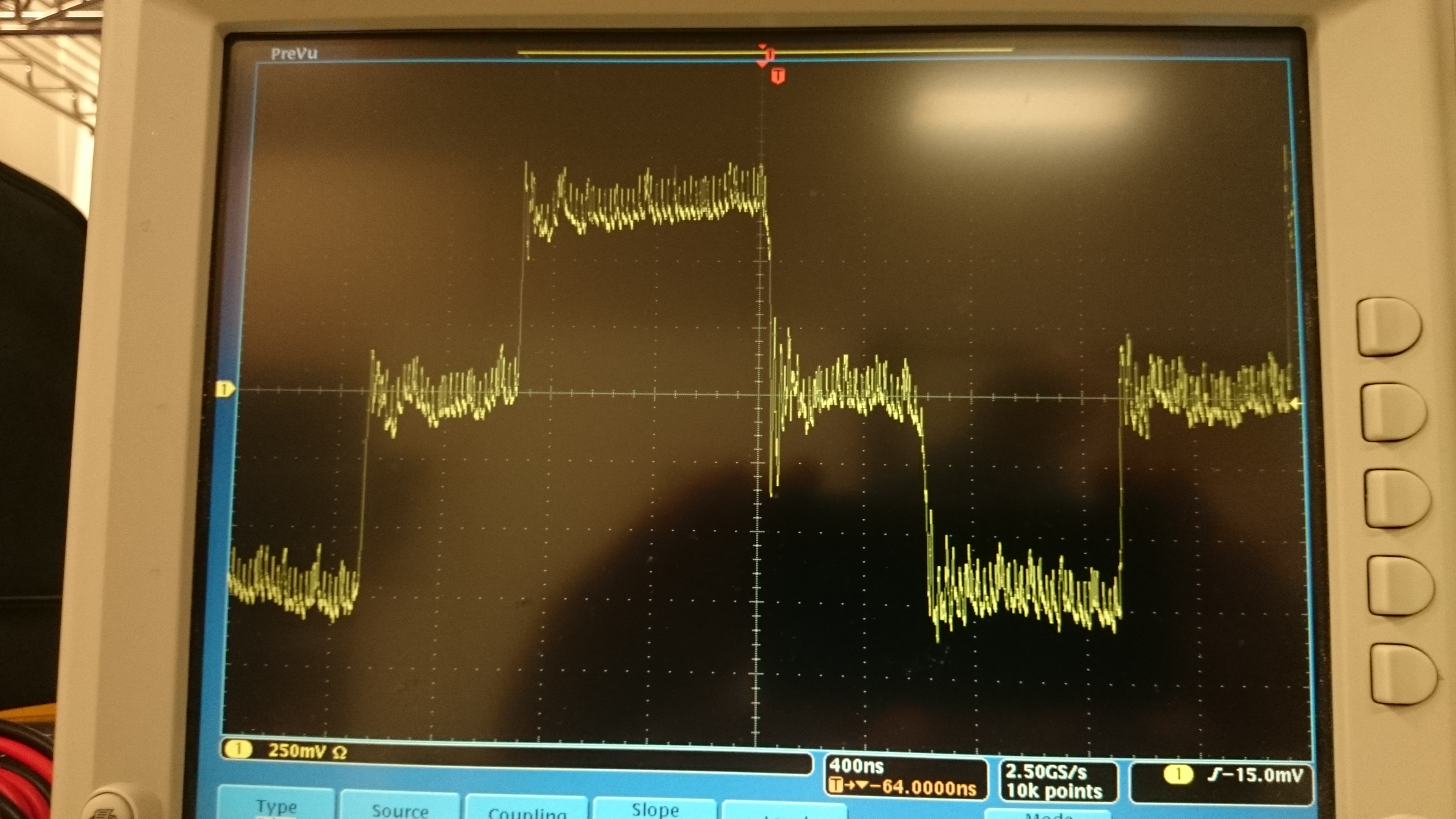
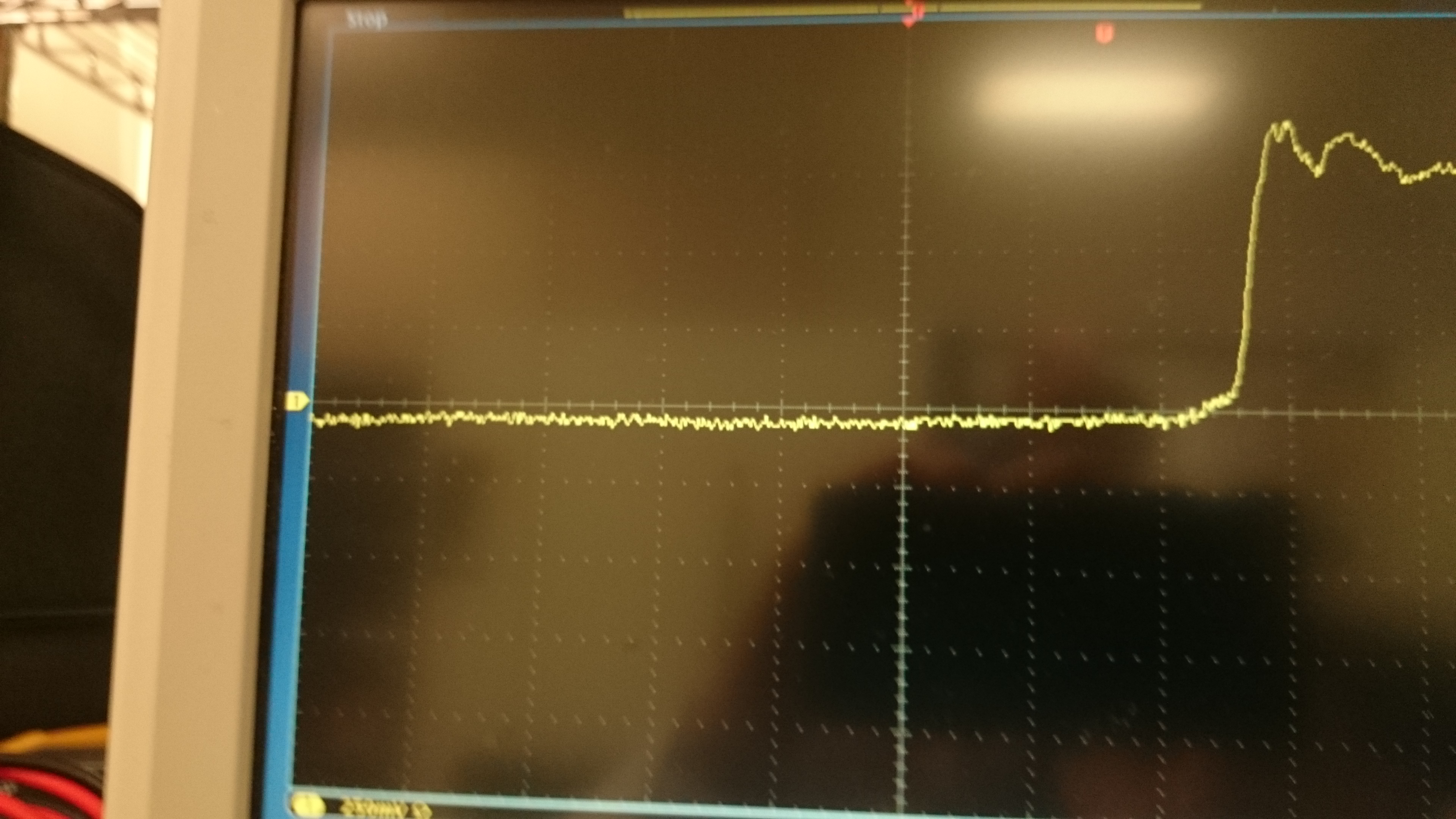
We have previously used the SN65DPHY440SS with a certain Omnivision CMOS Imager without issue (using lane 2).  Recently the same circuit (different layout) was added to another board, but used Lane 0 instead, and does not work.  I scoped the clock and data signals with a differential probe on each side of the SN65DPHY440SS and saw that clock looked correct on both sides, but only LP data seemed to be crossing on the output of Lane0.  On the input of Lane0, I could see the HS data, but the signal was strange in that with a differential probe across DA0P & DA0N, I saw signal on three different voltage levels, centered at 750mV, 0V, and -750mV.  See enclosed scope captures (each taken at different times).  Any thoughts as to what is going on here?
  • Hi John,

    Lane 0 has the DSI back channel. My guess is the DB0 output is not connected to a compliant DPHY Rx. It maybe connected to a FPGA.

    Regards
  • Joel,

    Yes, it is connected to an FPGA, but the interface as implemented, according to Lattice, is complaint with MIPI D-PHY specification v1.1 and DSI/CSI-2 specification v1.1. 

    I was able to do a couple of tests, and found that doing a cut/jumper job to move  from Lane0 to Lane1 fixes the problem, so yes, it appears tied to the DSI backchannel somehow

    Thanks,

    John

  • DPHY440’s LP TX is expecting to connect to an unterminated LP RX. With Lane 0 path (DA0P/N and DB0P/N) supporting bi-directional LP signaling, it is very important that DB0P/N LP TX is connected to an unterminated LP RX. If DB0P/N LP TX is connected to a HS RX, then LP signaling will not be able to reach the LP11 levels and which will cause the DPHY440 to not enable HS data path on Lane0.

    Try following for enabling lane0 HS path:

    Enable HS path for Lane 0 only:
    Write Register 0x50 with 8’h01 //Override enable for HS TX path
    Write Register 0x51 with 8’h01 //HS TX path enabled.
    Write Register 0x61 with 8’h00 // Disable LP path.
    Write Register 0x70 with 8’h01 //Override enable for HS RX path
    Write Register 0x71 with 8’h01 // HS RX path enabled.

    Bit 0 is lane 0
  • Joel,

         Thank you so very much for the register values;  we tried them out and it makes Lane0 work now.

    Regards,

    John