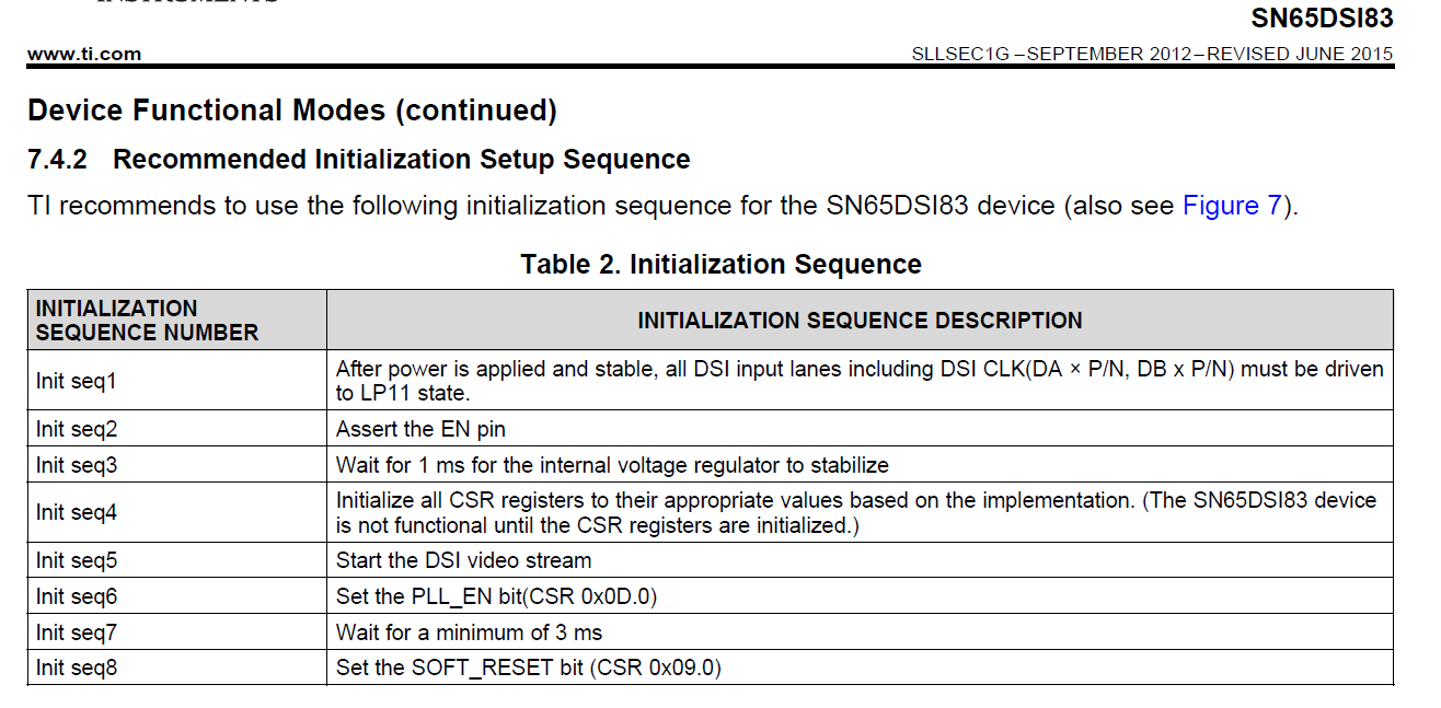
Part Number: SN65DSI83
Tool/software: Linux
Hi TI Experts,
We are debugging a Android PAD project for our customer.
This project is an variation from former design. In previous design, the CPU is Qualcomm MSM8939, and the LCD display uses a MIPI DSI interface, everything works fine.
The new design changed the LCD display interface into LVDS(Flat-link) . So the connection is MSM8939 -> SN65DSI83 -> LVDS LCD display. And the SN65DSI83 uses MIPI D-PHY clock as the clock source.
We've made great efforts to make the LCD display to work. We've been testing the hardware by using the test pattern feature of SN65DSI83, finally by changing the D-PHY clock to continuous mode, we succeeded. The test pattern from SN65DSI83 is as follows:
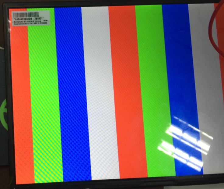
By seeing the test pattern, we believe that the clock is OK(we uses an oscilloscope to show the clocks from D-PHY and LVDS, both to be correct), the parameters of the LCD display is matched. however, we still cannot see any outputs in the LCD by switch the test pattern feature off. The timing parameter of the MIPI DSI has been reviewed, and seems to be good.
The LCD resolution is 1280x800, the MIPI D-PHY clock is 200MHz, and in our settings, we divided it by 4 as the LVDS clock.
The SN65DSI83 register setting for the test pattern to work is written in a HTML script and can be found in the attachment.
Please give some advice, is there somthing else should be considered?
<adapter>
    <configure i2c="1" spi="1" gpio="0" tpower="1" pullups="1"/>
    <i2c_bitrate khz="100"/>

	<i2c_write addr="0x2d" count="2" radix="16" nostop="1">00 08</i2c_write>
    <i2c_read addr="0x2d" count="9"/>
	<sleep ms="10"/>

	<i2c_write addr="0x2d" count="2" radix="16">09 00</i2c_write>

	<!-- Clock Source: bit0 = 1 using MIPI clock 37.5MHz ~ 62.5MHz -->
	<!-- <i2c_write addr="0x2d" count="2" radix="16">0A 03</i2c_write> -->
	<!-- DSI_CLK_DEVIDER = 4, so if D-PHY clock is 200MHz, LVDS clock is 50MHz -->
	<!-- <i2c_write addr="0x2d" count="2" radix="16">0B 18</i2c_write> -->

	<!-- Clock Source: bit0 = 1 using MIPI clock 25MHz ~ 37.5MHz -->
	<i2c_write addr="0x2d" count="2" radix="16">0A 01</i2c_write>
	<!-- DSI_CLK_DEVIDER = 8, so if D-PHY clock is 200MHz, LVDS clock is 25MHz -->
	<i2c_write addr="0x2d" count="2" radix="16">0B 38</i2c_write>

	<i2c_write addr="0x2d" count="2" radix="16">0D 00</i2c_write>

	<i2c_write addr="0x2d" count="2" radix="16">10 26</i2c_write>
	<i2c_write addr="0x2d" count="2" radix="16">11 00</i2c_write>
	<!-- CH_DSI_CLK_RANGE is 0x28 means 200MHz to 205MHz -->
	<i2c_write addr="0x2d" count="2" radix="16">12 28</i2c_write>
	<i2c_write addr="0x2d" count="2" radix="16">13 00</i2c_write>
	<!-- Data format: 24bit Format 1, DE,H-Sync, V-Sync, all positive polarity -->
	<i2c_write addr="0x2d" count="2" radix="16">18 7A</i2c_write>
	<!-- Increase differential output voltage swing for LVDS channel A.-->
	<i2c_write addr="0x2d" count="2" radix="16">19 08</i2c_write>
	<i2c_write addr="0x2d" count="2" radix="16">1A 03</i2c_write>
	<i2c_write addr="0x2d" count="2" radix="16">1B 00</i2c_write>

	<i2c_write addr="0x2d" count="2" radix="16">20 00</i2c_write>
	<i2c_write addr="0x2d" count="2" radix="16">21 05</i2c_write>
	<i2c_write addr="0x2d" count="2" radix="16">22 00</i2c_write>
	<i2c_write addr="0x2d" count="2" radix="16">23 00</i2c_write>
	<i2c_write addr="0x2d" count="2" radix="16">24 20</i2c_write>
	<i2c_write addr="0x2d" count="2" radix="16">25 03</i2c_write>
	<i2c_write addr="0x2d" count="2" radix="16">26 00</i2c_write>
	<i2c_write addr="0x2d" count="2" radix="16">27 00</i2c_write>
	<i2c_write addr="0x2d" count="2" radix="16">28 20</i2c_write>
	<i2c_write addr="0x2d" count="2" radix="16">29 39</i2c_write>
	<i2c_write addr="0x2d" count="2" radix="16">2A 00</i2c_write>
	<i2c_write addr="0x2d" count="2" radix="16">2B 00</i2c_write>
	<i2c_write addr="0x2d" count="2" radix="16">2C 0A</i2c_write>
	<i2c_write addr="0x2d" count="2" radix="16">2D 00</i2c_write>
	<i2c_write addr="0x2d" count="2" radix="16">2E 00</i2c_write>
	<i2c_write addr="0x2d" count="2" radix="16">2F 00</i2c_write>

	<i2c_write addr="0x2d" count="2" radix="16">30 02</i2c_write>
	<i2c_write addr="0x2d" count="2" radix="16">31 00</i2c_write>
	<i2c_write addr="0x2d" count="2" radix="16">32 00</i2c_write>
	<i2c_write addr="0x2d" count="2" radix="16">33 00</i2c_write>
	<i2c_write addr="0x2d" count="2" radix="16">34 23</i2c_write>
	<i2c_write addr="0x2d" count="2" radix="16">35 00</i2c_write>
	<i2c_write addr="0x2d" count="2" radix="16">36 03</i2c_write>
	<i2c_write addr="0x2d" count="2" radix="16">37 00</i2c_write>
	<i2c_write addr="0x2d" count="2" radix="16">38 23</i2c_write>
	<i2c_write addr="0x2d" count="2" radix="16">39 00</i2c_write>
	<i2c_write addr="0x2d" count="2" radix="16">3A 05</i2c_write>
	<i2c_write addr="0x2d" count="2" radix="16">3B 00</i2c_write>
	<!-- Enable LVDS CHA_TEST_PATTERN generation  -->
	<i2c_write addr="0x2d" count="2" radix="16">3C 10</i2c_write>

	<i2c_write addr="0x2d" count="2" radix="16">3D 00</i2c_write>
	<i2c_write addr="0x2d" count="2" radix="16">3E 00</i2c_write>

	<i2c_write addr="0x2d" count="2" radix="16">0D 01</i2c_write>
	<sleep ms="10"/>
	<i2c_write addr="0x2d" count="2" radix="16">09 01</i2c_write>


	<!--     <i2c_write addr="0x50" count="2" radix="16">00 00</i2c_write>
    <sleep ms="10"/>
    <i2c_write addr="0x50" count="2" radix="16">01 01</i2c_write>
    <sleep ms="10"/>
    <i2c_write addr="0x50" count="2" radix="16">FF FF</i2c_write>
    <sleep ms="10"/> -->


</adapter>