This thread has been locked.

If you have a related question, please click the "Ask a related question" button in the top right corner. The newly created question will be automatically linked to this question.

TPS65982: TPS65982

Part Number: TPS65982


Hi All, can you please help me with the below clarifications on TPS65982

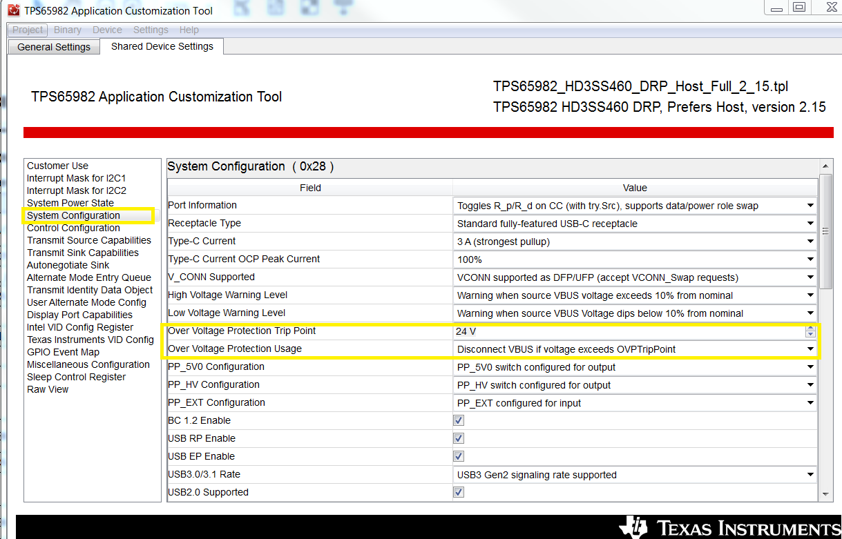
  • Does this device also have features like a surge stopper?
  • Can you share some presentation / short descriptive content which highlights the main function blocks of  this device
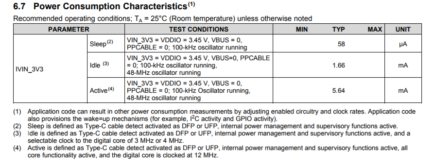
  • No load power consumption
  • Which are the internally generated supplies for this part?
  • Can you please give some idea on USB host programming for this?
  • Does it support USB host programming feature ?
  • Any power supply sequencing requirement for this part ?

regards 

  • Hi Siddharth,

    * This device has an overcurrent limiter.

    * Main Features: Fully integrate USB Type-C and PD solution, Compliant to the USB Type-C 1.x and USB PD 2.x specs, Integrated high speed mux and alternate mode support, flexible system interface, Integrated USB Endpoint w USB2.0 Flash Update and Billboarding, Supports 2 Internal power path (up to 3A each) and 1 External Power Path (up to 5A).

    *Power consumption can be found in the datasheet under Section 6.7.

    * From Section 6.5 in the TPS65982 datasheet

    * USB Host Interface programming is supported can be done with our Application CustomizationTool. With the tool, there are default configurations already pre-defined that any user can use to modify to fit any application. This tool is used to read and write to any register. More information and features can be found in the TPS6598x Application Customization Tool User Guide

    * Power supply sequencing is not required.

  • Thanks can you please also let me know which are the pins that have internal pull up & pull down resistors & of what value?
  • Hi Jamie can we discuss this offline , can you please contact me at my email id ? or share the same with me ?
  • Hi can anyone help on this topic? can you please also let me know which are the pins that have internal pull up & pull down resistors & of what value?
  • Hi Siddharth,

    pins GPIO0-GPIO17 have configurable pull-up/pull-downs internal. These pull-up/pull-downs can be enabled or disabled through the application customization tool. The typical value of the pull-up/pull-down resistance is 100k.

    Thank you,
    Eric
  • thanks for the reply. can you please share the link for application customization tool

    - can you please also confirm how is the ILIM , the current limit setting being done. is it completely programmable by software or has any transfer function being implemented through external components on any of the pins

    - can you please clarify what is the Gate control mechanism for the PPHV to VBUS path internal fets ,what i feel is that over current causes the gate to be turned off , is that correct ? and what in case of an over voltage and case when there is no input voltage say for PPHV = 0

    - similarly for PP_5V0

    - what is the Fast current limit 

    - what is the value of VREV5V0 & VREVHV?

    - on figure 49, there is an enable signal for each LDO like LDO_3V3_VB_EN, are these coming out on any of the pins?

    - VDDIO  is source for which of the  pins?

    thanks

  • - Here is a link to the config tool: www.ti.com/.../tps6598x-config

    - The current limit is set internally by software.

    - The device will turn off the external FETs for OCP, OVP, UVP, or OTP events.

    - Same applies to PP_5V0

    - What do you mean with fast current limit?

    - These values are found on pg 17 of the datasheet: www.ti.com/.../tps65982.pdf

    - No, these signals are internal to the device

    - VDDIO is VDD for I/O. Some I/Os are reconfigurable to be powered from VDDIO instead of LDO_3V3. When VDDIO is not used, tie pin to LDO_3V3. When not tied to LDO_3V3 and used as a supply input, bypass with capacitance CVDDIO to GND. You can read more about VDDIO in section 10.3 of the datasheet.

    Thank you,
    Eric
  • thanks for the reply,

    for VDDIO i read what you mentioned but what i am requesting is which are the IO pins that can be configured to be supplied from VDDIO?

    - in most of the block diagrams there is a fast current limit symbol , for example please see Figure 86
    - can you please elaborate a bit on UVP , OVP scenarios for turning off the FET
    - Output switch resistance from VIN_3V3 to VOUT_3V3 is 0.35ohm, is this the FET resistance
  • thanks for the reply

    VREV5V0 threshold is 10mV, so as per figure 21 , if Vbus increases VPP5V0 by 10mV the path FET diode will breakdown to conduct current?
  • Hi All, request your feedback . regards
  • in continuation to my previous questions request clarification again -on -For the path from PPHV TO VBUS as well as PP5V0 to VBUS there is a fast current limit indication. what does that constitute and how is the OVP getting accomplished for the FETs along the path from PPHV TO VBUS?
  • in continuation to my previous questions how are GPIO 0/1 interfaced and in what condition will these be pulled up to supply? as i see that these can be pulled up to LDO3V3 , is that correct?
    similarly for USB2P & USB2N
  • Hi Siddharth,

    GPIO0/1 can be configured in the Application Customization tool in the GPIO Event Map (Register 0x5c).

    It is dependent upon user's desired configuration whether the internal pull up/ down are enabled.

    As far as GPIO0/1 is concerned, it can be referenced in Table 8 of the TPS65982 datasheet that the GPO0/1 are connected to LDO_3V3.

    Regards,

    Jimmy Hua

  • Hi Siddharth,

    The OVP threshold on VBUS is between 5V-24V(Section 6.6 in datasheet)  and is set in register 0x28 System Configuration by using the Application Customization tool.

    Regards,

    Jimmy Hua

  • thanks for the reply but i was requesting is procedure by which the gate of the internal FETs along the PPHV to VBUS path are being controlled in case of an over voltage. also i see a fast current limit along these paths ,how is that controlling these FETs?