This thread has been locked.

If you have a related question, please click the "Ask a related question" button in the top right corner. The newly created question will be automatically linked to this question.

TPS65981: TPS65981 PD Controller ADC and Debug

Part Number: TPS65981
Hi,
 
We're planning to use TPS65981 PD Controller in our ongoing project and our device will function as Power sink only and Dual Role Data modes.
 
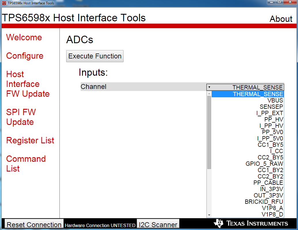
We suppose to monitor the current flow from the USB-C connector using the TPS65981 internal ADC. However, we see simply channel selection and read-out register bits on TRM. I'm not sure on the channel selection register bits value intended to select the PP_HV. Could you please provide us with ADCChan register bit description on selecting which input to be sensed? Also, the TPS6598x Application Customizer GUI has no such relative information on ADC read-out. Please support us with necessary documents. 
Inline image 1
Inline image 2
Also, we like to explore the TPS65981 programming through SWD interface. Please suggest us with the appropriate Debugger kit if any and provide us with user manuals to get started with the same.
 
Regards,
Manikandan M V
  • Hi Manikandan,

    You can use the internal ADC to read the SINK current on PP_HV using the TPS6598x Utilities GUI by using the ADCs command in the Command List tab. The ADCs channels are listed there with "Thermal_Sense" as channel 0. The channel for I_PP_HV would be channel 5.

    The TPS65981 will boot using a SPI Flash chip connected to it on the PCB. After the device has booted, it is possible to reconfigure some registers using the Host Interface commands over I2C. It does not support programming through SWD. 

    Thank you,
    Eric

  • Thank you, Eric. It seems we require USB-I2C host adaptor to work on it with our real time hardware and we order the same to get started with it.

    We would like to explore the TPS65981 programming through SWD interface. Please suggest us with the appropriate Debugger kit from TI if any.


    Likely, if we manually reset the TPS65981 (through MRESET pin) would it reboots and initiates the PD communication on CC lines? If I intend to reset the USB-C controller TPS65981 runtime on USB PD Sink Only device, it may result in power cycling. Is this understanding correct?


    Regards,

    Manikandan M V

  • Hi Manikandan,

    The device cannot be interfaced through the SWD pins. The firmware on the TPS65981 does not support it.

    MRESET can be used to reset a co-processor and is just passed through our device. This will only affect the RESETZ GPIO.

    Thank you,
    Eric
  • Hi Eric,

    Okay, we would like to understand the scope for SWD termination on TPS65981.

    Fine, understood.

    Our device would be a power sink only device at 5V/2A and 5V/3A modes as our board max. startup power requirement is 10W. We're using TPS65981 PD controller to function the same.

    Once we power-on TPS65981 through USB-C (5V), it has to route the power from VBUS to PP_HV if only 5V/2A or 5V/3A PD sourcing device is connected. Rather it should not work with the 5V/0.5A or 5V/0.9A from the SDP. To function accordingly, could you please share the detailed measures?

    Either we have to disable the VBUS power path (strapping BUSPOWERZ to 3.3V) and then giving control to application firmware to connect if defined PD sourcing device is connected or through configurable GPIOs? Hope I'm clear

    Currently, in our device we have tied BUSPOWERZ to 1.8V for power path strapping (as per the datasheet dead-battery state diagram) and under such case if we connect a PD sourcing device whether it routes only the high power (5V/2A or 5V/3A) from VBUS to PP_HV?

    Besides, can you review our device TPS65981 PD controller schematics?
  • Hi Manikandan,

    The SWD lines were added for debugging the internal FW on the TPS65981. We do not open this interface up to the user since the firmware is only meant to be configured and not rewritten.

    If I understand correctly, you want to boot your TPS65981 in dead battery mode and have 5V pass from VBUS to PPHV?
    If you have BUSPOWERZ tied to 1.8V then you will pass the 5V from VBUS to PPHV and then load your app configuration through SPI flash. If you have BUSPOWERZ tied to 3.3V then you will first load your app configuration from SPI flash before closing any of the power path switches.

    You can send me a personal message with your contact information for a schematic review.

    Thank you,
    Eric
  • Thank you, Eric.

    Just to be more clear, we tie BUSPOWERZ to 3.3V and the TPS65981 loads our custom application setting. We define sink PDO's 5V/2A & 5V/3A pass from VBUS to PP_HV in binary. Under such case, TPS65981 pass 5V power only if the configured sink PDO's are set? It won't pass nominal 5V/0.9A or different unconfigured sink PDO's are set on PD communication. Is this understanding correct?

    Our target is passing only 5V/2A and 5V/3A sink PDOs from VBUS to PP_HV path. Hope I'm clear.

    Thank you,

    Manikandan M V

  • Hi Manikandan,

    Yes your understanding is correct. With BUSPOWERZ tied to 3.3V, the TPS65981 will not pass power through the system until the application firmware is loaded and a PD contract is negotiated.

    Thank you,
    Eric
  • Hi Eric,

    Okay, thank you. Please let us know your email id for sharing Schematics and Layout review.

    Could you please share the reference manual for the commands found on TPS6598x Host Interface Tools GUI if any?

    Regards,

    Manikandan M V

  • Hi Manikandan,

    I will send you a personal message with my email address. You can find information on the 4CC commands in the Host Interface Technical Reference manual: www.ti.com/.../slvuan1a.pdf

    Thank you,
    Eric
  • Hi Eric,

    I'm expecting your ping with the email address for sharing design review.

    Also, I'm working on configuring the PD profiles as discussed above. I have configured 5V/2A sink profile using Application Customization tool and generated a .BIN (Low-Region only & Low-Region and Full Flash Image file types). Then, loaded this .BIN file into the TPS65983 Evaluation Module using Cheetah Flash Programmer. However, the 5V from VBUS is not passed to PP_HV while powering up using Google Pixel Charger Adaptor which is PD compliant upto 18W. Further probed on CC lines and observed some data flow activity on CC line. Sorry, I'm not sure whether I'm missing any measures.

    Thinking to execute our Board Bring-up as to generate a 5V/2A sink PD profile .BIN file and load them into the SPI Flash memory using Cheetah Flash Programmer. Could you please support us with an appropriate .BIN file and its process flow document?


    Regards,

    Manikandan M V

  • Hi Manikandan,

    I could not send you a private message. What is your email address?

    As far as programming your EVM, make sure you are using the Full Flash binary file. Also, after the SPI flashing is complete, make sure you disconnect your programmer and power cycle your EVM.

    Thank you,
    Eric
  • Hi Eric,
    Please drop a test mail to manikandan.mv@vvdntech.in for sharing design review.

    I have generated Full Flash Image .BIN and followed as you said. However, 5V is not passed from VBUS to PP_HV. Do you suggest any recommended USB PD compliant Sourcing devices for verifying our PD sink device functionality?

    Regards,
    Manikandan M V