This thread has been locked.

If you have a related question, please click the "Ask a related question" button in the top right corner. The newly created question will be automatically linked to this question.

HD3SS215: Asking for the HD3SS215 DP and HDMI application schematic

Part Number: HD3SS215

Hi Team,
Cusotmer would like to use HD3SS215 as DP and HDMI source switch.
here is the block diagram.

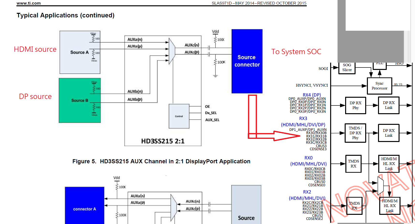
Which schematic that customer can follow for HDMI/DP switch application? figure 4 add the ac cap, but figure 7 do not add the ac cap.

Please provide your comment.


Thanks,
SHH

  • Hi SHH,

    This is a sink application, right?

    Is the SoC a receiver that can handle DP and HDMI video both AC coupled?

    Does it have separate ports for DDC and AUX?

    Regards

  • Hi Moises,

    Yes. it is sink application.

    for the questions you raise, you mean scalar need to have the following capability. Right? If scalar cannot support, then this application will not be workable.

    1. scalar need to support both HDMI and DP both AC coupled signals.

    2. Scalar need to have separated ports for DDC and AUX.

    Thanks,

    SHH

  • Hi SHH,

    DP is AC coupled while HDMI is DC coupled, I haven't seen a receiver that can handle the two kinds of signals.
    However, HDMI DC coupled can be made AC coupled adding resistors and capacitors, in this case, the same receiver like an FPGA could take AC coupled signals for both kinds of video protocols.
    Besides, HDMI has TMDS_CLK which is used to do clock recovery, while DP clock is recovered from Main Lanes.

    HDMI uses DDC, which is basically I2C working at 100kHz or 400kHz
    DP uses AUX, which is AC coupled standard data rate is 1Mbps and FAUX is 720Mbps
    I have seen transmitters for both DDC and AUX but not a receiver, this doesn't mean they don't exist.

    The customer has to verify their SoC can handle the two protocols.

    Regards