This thread has been locked.

If you have a related question, please click the "Ask a related question" button in the top right corner. The newly created question will be automatically linked to this question.

TFP401A: TFP401A to SN75LVDS83B connectivity

Part Number: TFP401A
Other Parts Discussed in Thread: SN75LVDS83B, , TFP401

Hi,

we need to convert HDMI to drive a LVDS panel (see attached datasheets of both display and controller

We are using the TFP401A together with the SN75LVDS83B. Please see the schematic below to see how we connected the two ICs.

Questions:

1) About connectivity between the two TI chips. According to the attached TI app notes and datasheets there are a number of different ways to connect the two TI chips to each other. It looks like that depends on the display driving pattern. But we could not make much sense. In our schematic you can see how we connected them together but we don’t think the way we connected them is correct because the data from a supplier shows a different configuration (but we only have partial information on that). So could you please show/let me know the correct connectivity to drive the attached display in both 6 bit and also in 8 bit configuration of the display.

2) Following from the above question, could you please explain more clearly the logic behind the connection between the two TI chips? Could you please explain it in detail.

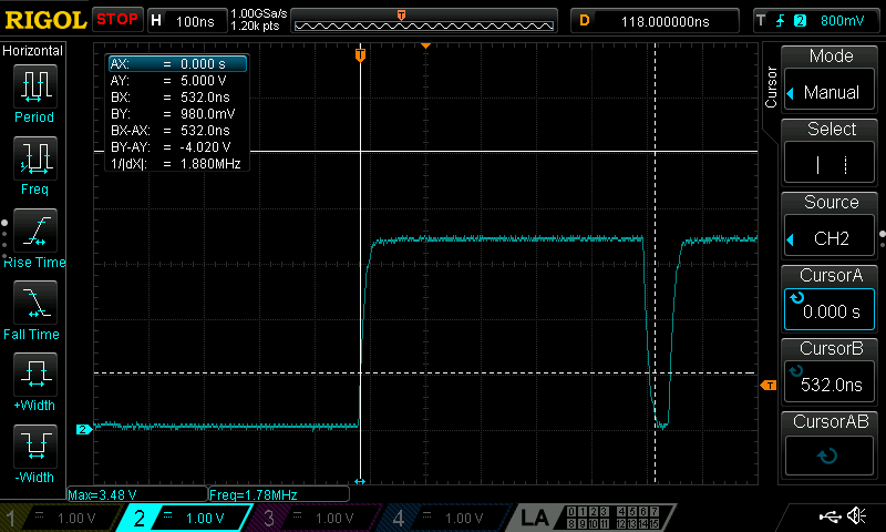
3) Also in terms of routing between the SN75LVDS83B and the TFP401, do the traces need to be routed with a controlled impedance?

4) if so, what is the maximum mismatch in trace length between all traces between the two chips?

Many thanks

Rick

HX8282.pdfER-TFT070-3_Datasheet.pdf

  • Hello Rick,

    For 8 bit configuration follow the connection described in the Figure 3.  1-Channel LVDS Connection Example.

    For 6 bit configuration the lane Y3 is not used. That means, the following inputs are not used: D23, D17, D16, D11, D10, D5 and D27.

    The trace length of data and control signals out of the receiver should be kept as close to equal as possible. Trace separation should be ~5X Height. As a general rule, traces also should be less than 2.8 inches if possible (longer traces can be acceptable).

    For the connection between the two TI chips please follow the suggestions on the 10.2.2.1 Data and Control Signals section in the TFP401 datasheet.

    Regards

  • Thank you Joel,
    just to be sure, when you say ~5x Height you mean vertical gap between the bottom surface of the trace and the top surface of the plane below it, correct?

    Also is there a document explaining the order in which the TFP401A serialises? i.e. the serialisation sequence from input to output... i.e. RX0-RX3 paralleled out every clock? Or every 4 clocks? or in reverse order? etc. I assume it should be on the datasheet but cannot find it.

    Thanks
    Riccardo
  • Hello Riccardo,

    It refers to the trace thickness.

    Regarding the data synchronization, you can find all the details In the section 9.3.2 TFP401/401A Clocking and Data Synchronization.

  • Hi Joel,

    I know you were referring to the trace width, but I was referring to the "height". By height you mean the vertical gap between the bottom surface of the trace and the top surface of the plane below it, correct?
    Thank you

    Rick
  • Also forgot... when you say trace separation do you mean between pairs or between two traces of the same pair?
    Thanks
    Rick
  • Hello Rick,
    Yes, you are correct in the height. Also, the trace separation is between the parallel data and control signals.
    Regards
  • Thanks Joel,

    we have now made a board as per your guidelines above (we use a 8-bit display config) but there is no video signal.

    Could you please check the attached schematic especially:

    1. the connection between the TFP401A and the SN75LVDS83B

    2. the configuration of both of the above ICs

    3. the connections as mentioned in point 1 above considering the IC datasheet of the display we are using (attached PDF)

    Many thanks

    Rick


    HDMI to LVDS - Variant 1.pdf

    HX8282 (1).pdf

  • Hello Rick,

    What panel resolution/ clock frequency are you using?

    Do you have the PDO# and PD terminals controlled by GPIOs?

    Regards
  • Hello Joel,

    the resolution is 1024 x 600, please find attached the display datasheet in case you need further info/details. The controller (in caase you need to know the signals pattern/sequence) is the HX8282 (pdf also attached).

    Both PDO# and PD are left unconnected (as you can see from the schematic neither pull up nor pull down are assembled).

    We left them floating because they have internal pullup and when high they are in normal operation.

    Thank you

    Rick

    5684.HX8282 (1).pdf

    8321.ER-TFT070-3_Datasheet.pdf

  • Rick,
    Could you measure the ODCK, VSYNC, HSYNC, and DE frequency of the TFP401?
    Regards
  • Hi Joel,

    VSYNC is a steady 0V

    HSYNC is a steady 3V3

    DE  is a steady 3V3

    ODCK please see the two attached scope screenshots (one freeze frame and one running). The one showing a running trace shows a lot of jitter. The frequency seems around 1.8MHz BUT (!!) the scope we have is only 1GSps - 100MHz so if the clock is a lot higher the jitter in the screenshot might be due to the scope limitation in the waveform acquisition.

    Few questions:

    1. what frequencies should we expect on all 4 signals you asked about?

    2. I assume VSYNC HSYNC and DE should contiuously switch between 1 and 0 even if the display has a still image (which is our case - although we clearly do not see any images because the display path clearly not working). Is that correct?

    3. if so what could be the reasons? We checked all the PCB side of things for ICs pin numbering mapping and similar potential connectivity issues but they are all as per datasheets.

    4. is the connectivity/wiring between the 2 chips correct considering all the following (I attached all datasheets in previous posts):

    - for the display driver IC required LVDS driving/communication pattern/sequence

    - display resolution

    - anything else

    5. is the configuration of both ICs correct (as per schematic showing which configuration pull-ups/down have been installed on the board and which have not)?

    Please find scope traces screenshot below:

    Many thanks

    Rick

  • Hello Rick,

    The TFP401 looks configured correctly in the schematics. It seems that your hdmi source is not sendding data to the TFP401. With no input, the device will output the free-running PLL on ODCK. With no input, the state of the control and data output signals is unknown.
    Keep in mind that the TFP401 is not involved in the EDID communication, the EDID information will flow directly from the Display to the graphics controller through the DDC lines. If you HDMI source needs to know the EDID information to start the video transmission you need to have an EDID ROM to store the display information, this is for example how the PC knows the capabilities of the sink.

    Regards
  • Hi Joel,
    the HDMI source is a Raspberry PI compute module so it sends out a standard HDMI signal and all infos required are already coded in the standard Raspberry Pi OS driver.

    When the same compute module is installed in the standard Raspberry Pi IO board the display works correctly (it is a direct HDMI connection to a monitor). In both cases (the Compute Module standard board and our PCB) the only connection between the Compute Module and the display (or the TFP401A) are just the 4 differential pairs. So in both cases the exact same signals are sent through and the only communication occurs on those 4 HDMI differential pairs.

    What can it be?
  • Rick,

    Could please share the Rasperry Pi and compute models that you are using?

    Additionally, please share an scope capture of the HDMI clk provided by your source.

    Regards
  • Hi Joel,
    The Rasp Pi Compute Module we use is the latest version (CM 3).

    We tried probing the trace but for as bizarre as it might seem no signal appears, neither on our board nor on the official Compute Module IO board with the display up and running with full image displayed. The signal should be few hundreds mV amplitude but no matter what we try.
    We tried:
    - a single scope probe on either one of the clock differential lines with the scope referenced to GND (i.e. probe clip to the board ground)
    - 2 probes with ground clip connected together (and not to the PCB GND) and probing the two differential clock signal lines one with each probe with the scope on differential and also on math (difference)
    Probably because as mentioned previously all our scopes are 100MHz?

    Thank you

    Rick

  • Rick,

    Based on the documentation I found online, the compute module you mention has the following signals:

    HDMI SCL
    HDMI SDA
    HDMI CEC
    HDMI CLKx
    HDMI Dx
    HDMI HPD N 1V8

    It seems that this module requires knowing the sink capabilities in order to be able to output the correct resolution that matches your LCD screen.

    The TFP401 is not really involved in the EDID exchange (or HDMI_SCL & HDMI_SDA) . Therefore, you need to connect an external EDID ROM to store the display information this is how the your module knows the capabilities of the sink.

    Regards
  • Hi Joel,

    we got it working by defining a custom monitor (by creating a custom descriptor in the config.txt file).

    Thanks