Part Number: TUSB1310A
Hi TI support team,
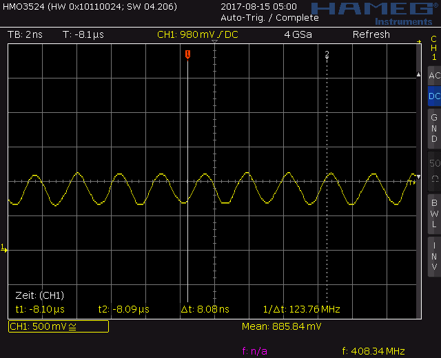
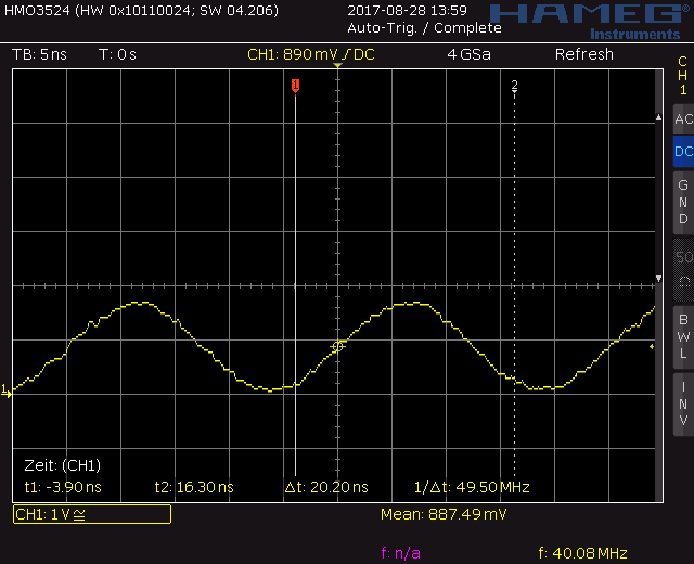
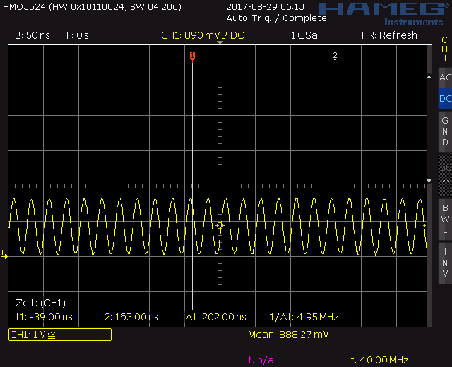
I have encountered a problem while debugging my TUSB1310A design. First of all I wanted to measure the PCLK. For that reason, I have booted up the system and then the PCLK was 250 MHz. But against to your documentation, the clock was 900 mV /- 100 mV. Could this be correct? In the documentation I found, that the clock should meet the LVCMOS18 standard. Do you know, where the problem is?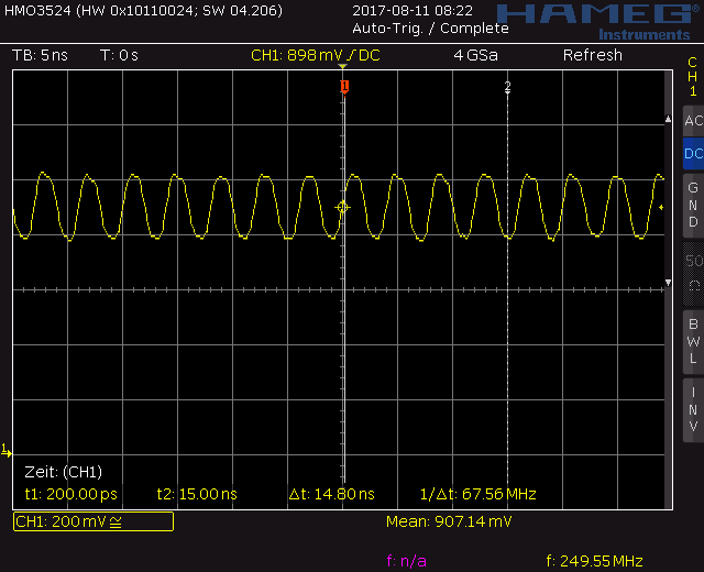
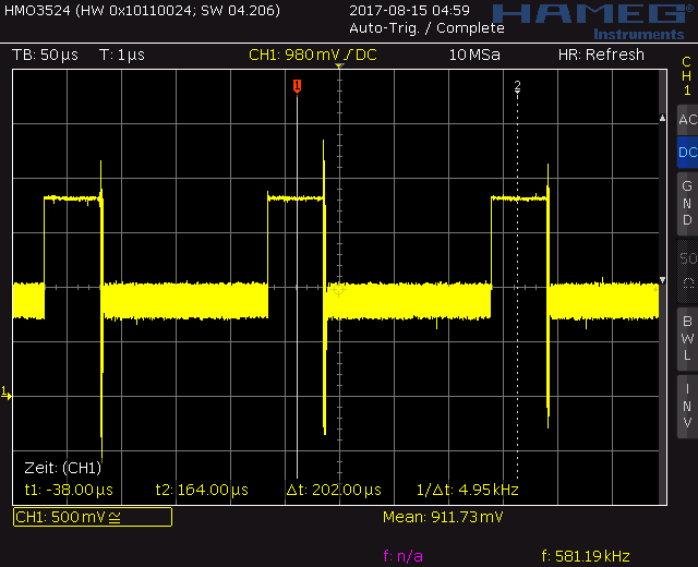
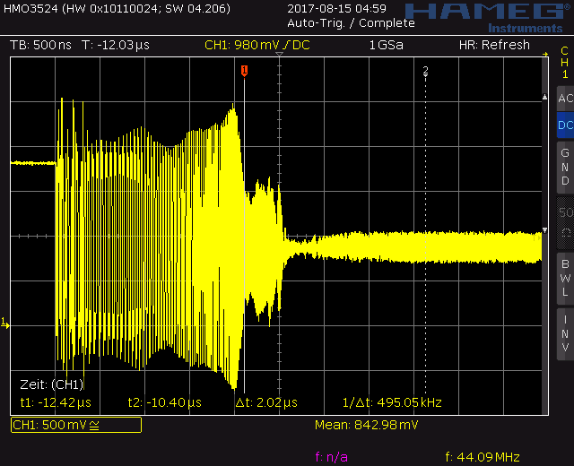
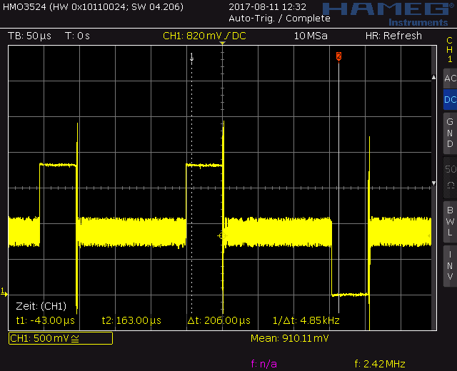
After a few minutes, the PCLK was getting unstable in the follwing way: The clock is “stable” for 150 µs as described at first (250 MHz, 900 mV /- 100 mV), than it is high (1.8V) for 50 µs. This is periodically. So the “stable” part for 150 µs follows the high part for 50 µs and so on:
Here is the schematic:

The DIP switches are used in the following way:
S1 – 1 -> ON
S1 – 2 -> OFF
S1 – 3 -> ON
S1 – 4 -> OFF
S2 – 1..8 -> OFF
S2 – 9 -> ON
S2 – 10 -> OFF
All signals connected to page 3 are connected to an FPGA. The signals in the FPGA are connected in the following way:
USB3_USB3_1_POWER_DOWN0 <= '0';
USB3_USB3_1_RESETN <= ‘1’;
USB3_USB3_1_OUT_ENABLE <= '1';
USB3_USB3_1_NEN_P5V0_OUT <= '0';
There are 2 of the TUSB1310A Chips on one board. Both Chips show the same behavior.
Thanks and regards
Michael