This thread has been locked.

If you have a related question, please click the "Ask a related question" button in the top right corner. The newly created question will be automatically linked to this question.

SN65LVCP418: Asking for the SN65LVCP418 design support

Part Number: SN65LVCP418

Hi Team,
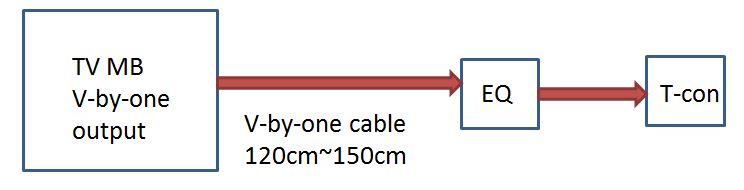
Customer would like to use SN65LVCP418 to implement the demo.
Here is the block diagram.
Could you please provide your comment for this block diagram? 

customer has questions about SN65LVCP418 as below
1.VCC、RESN、I2C_EN sequence?
2.RESN active:internal or external ?
If external , RESN pin from high to low , need to be keep low or high?


Thanks,
SHH

  • Hi SHH,

    For the VCC, I2C, and RESN pins.

    I recommend to allow VCC and I2C to ramp up together.  Delay the ability of RESN to ramp to a high level using active or simple RC control over the input voltage.  This will enable the I2C mode and reset the 418 registers.

    RESN is an active "Low" signal.  There should be a 35KOhm pull-up inside the device. An external capacitor to GND would provide a delay function and reset the registers.  After the initial reset, the pin can remain "High".

    Regards,

    Lee

  • Hi Lee,

    How to connect pin 16?

    Thanks,

    SHH

  • SHH,

    Ideally the SN65LVCP418 would operate with AC coupled inputs and allow the VBB pin to self-bias to 1.6V

    If DC coupling is required then the VBB pin can be connected to a voltage between 1.5V and  (VCC-VID/2).

    What is the common mode of the V-by-one output?

    Regards,

    Lee

  • Hi Lee,
    Thanks for help. Customer has question for the VBB. please help.
    V-by–one data channel consists of AC-coupled and terminated differential pairs.
    Q:
    1. VBB is internal voltage of SN65LVCP418 or needs external input 1.6V?
    2. How about the power consumption if it needs external voltage?
    3. Can customer use divider resistance to keep 1.6V?

    Thanks,
    SHH

  • Hi SHH,

    Since the channel is already AC coupled the VBB can be left disconnected and the internal circuits will keep the common mode at 1.6V.

    There is not requirement to add an external voltage divider to drive the VBB pin.

    Regards,

    Lee

  • Hi Lee,

    Could you help review the schematic? The password is"ti".

    https://e2e.ti.com/cfs-file/__key/communityserver-discussions-components-files/138/CONVERTOR-BOARD_5F00_20170831.7z

    Thanks,

    SHH

  • Hi SHH,

    I would recommend using adding a pull-up / pull-down resistor network on the RESN and VBB inputs.  I think to start with these resistor networks would be NC to start with in the BOM.

    Regards,

    Lee