This thread has been locked.

If you have a related question, please click the "Ask a related question" button in the top right corner. The newly created question will be automatically linked to this question.

TMDS181: about TMDS181

Part Number: TMDS181

Hi dear supporting team,

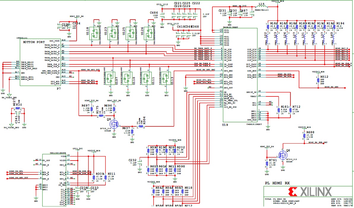
my customer is evaluating XILINX evk with TMDS181 on it, the setup is camera input to TMDS181, and then to FPGA.  the sch is as attached. 

while they found there is no output even there is singal input to our chip.  and they are running at HDMI2.0, TMDS181 powering up with default setting. 

pls help comment which regs need be changed. tks!

regisiter address offset(hex)   |   value(hex)

0x0                                   0x54

0x1                                   0x4D

0x2                                   0x44

0x3                                   0x53

0x4                                   0x31

0x5                                   0x38

0x6                                   0x31

0x7                                   0x20

0x8                                   0x1

0x9                                   0x2

0xA                                   0xB1

0xB                                   0x0

0xC                                   0x0

0xD                                   0x0

0xE                                   0x0

0xF                                   0xF

0x10                                  0x0

0x11                                  0x0

0x12                                  0x0

0x13                                  0x0

0x14                                  0x0

0x15                                  0x0

0x16                                  0x0

0x17                                  0xF0

0x18                                  0x0

0x19                                  0x0

0x1A                                  0x0

0x1B                                  0x0

0x1C                                  0x0

0x1D                                  0x0

0x1E                                  0x0

0x1F                                  0x0

0x20                                  0x4A

  • Hi Vera,

    The registers values are the default and the schematic looks fine.

    Could you apply Rx and Tx changes? this is writing a 1 to register 0x0A[2]?

    Could you share the register from page 1?

    Regards

  • hi Moises,

    thanks for reply!

    after writing 1 to 0x0A[2], the readout for all the reg is as below:

    Register offset(hex)             Value(hex)

    0x00                                 0x54

    0x01                                 0x4D

    0x02                                 0x44

    0x03                                 0x53

    0x04                                 0x31

    0x05                                 0x38

    0x06                                 0x31

    0x07                                 0x20

    0x08                                 0x1

    0x09                                 0x2

    0x0A                                 0xB1

    0x0B                                 0x0

    0x0C                                 0x0

    0x0D                                 0x0

    0x0E                                 0x0

    0x0F                                 0xF

    0x10                                 0x0

    0x11                                 0x0

    0x12                                 0x0

    0x13                                 0x0

    0x14                                 0x0

    0x15                                 0x0

    0x16                                 0x0

    0x17                                 0xF0

    0x18                                 0x0

    0x19                                 0x0

    0x1A                                 0x0

    0x1B                                 0x0

    0x1C                                 0x0

    0x1D                                 0x0

    0x1E                                 0x0

    0x1F                                 0x0

    0x20                                 0x8A


  • Hi Vera,

    The registers look the same, I guess writing 0x0A[2] didn't have any effect, right?
    Can you see the display listed in the PC?
    Could you write register 0xFF=0x01, then read all the registers, at the end write back 0xFF=0x00.
    Please share the registers after this procedure, you can attach the file to save space.

    REgards