This thread has been locked.

If you have a related question, please click the "Ask a related question" button in the top right corner. The newly created question will be automatically linked to this question.

TUSB1002: TUSB1002 10G Application architecture diagram question

Part Number: TUSB1002


Hello.

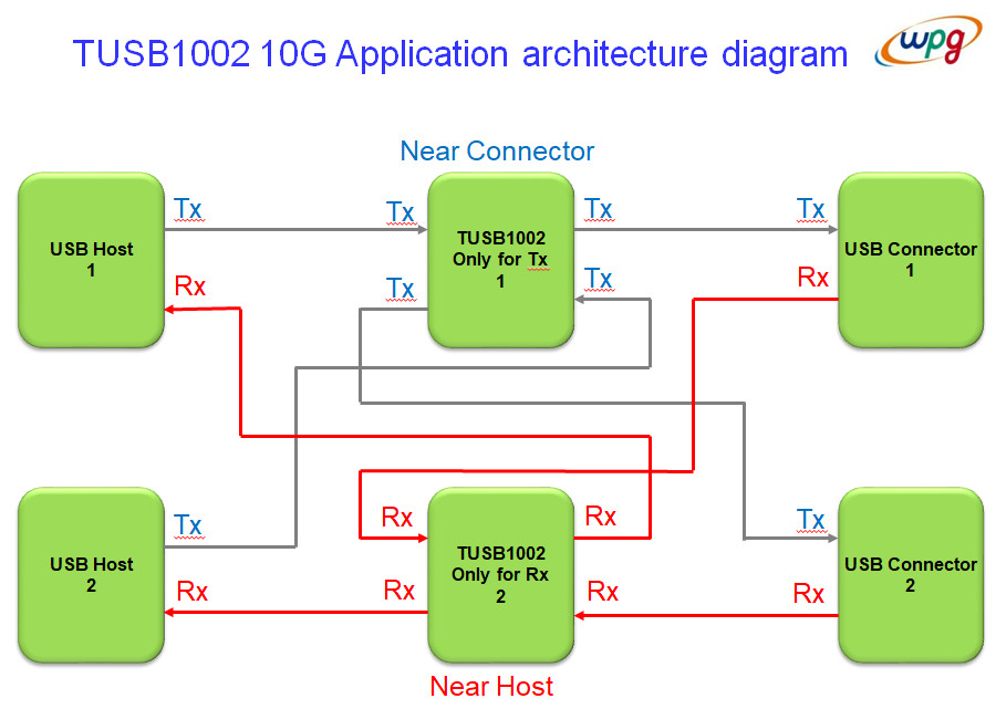
We have a project used two TUSB1002 for two USB ports. One TUSB1002 only for TX and other one TUSB1002 is only to RX. Like below diagram. We have some question need you help on below. Thanks~
1. Have any customer use below architecture diagram for project?
2. USB Rx/Tx whether the differential signal needs the same length?
3. USB Pre-channel can we less than 6 inch? maybe like 3.5 inch. and Post-channel length can we greater than 0.5 inch? we will less than 2 inch in length. Please reference Figure 17-3 from Intel PDG.
4. In this architecture diagram can we pass USB test? like LFPS. When I set SLP_S0# to 0.
5. In this architecture diagram how should I set the MODE and SLP_S0 # pins?
6. TUSB1002 Pin14 SLP_S0# function is Receiver Detect Control or sleep mode control?

  • Hello AJ,

    The connection described in the diagram is not supported by the TUSB1002. Why the customer wants to use such connection. No customer has used it.

    We recommend having the RX and TX differential pairs matched but it is not mandatory since TX & RX paths are independent per USB3.1 protocol.

    The lengths you mentioned are short, we recommend to use a re-driver when the channel is >5 inches. For this case, I recommend configuring the TUSB1002 with low EQ levels.

    The connection is not supported and it is almost certain that it will fail compliance testing.

    Do not use this connection.

    Best regards,
    Diego.
  • Dear Diego.
    Thanks so much for you kindly help it.