This thread has been locked.

If you have a related question, please click the "Ask a related question" button in the top right corner. The newly created question will be automatically linked to this question.

DS80PCI810: Best placement for repeater location

Part Number: DS80PCI810
Other Parts Discussed in Thread: DS80PCI800

Hi there:

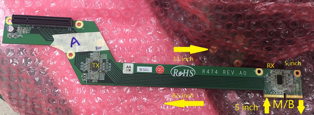
I'm helping customer to debug the DS80PCI810 performance in server's add-in card.

We found sometime the card will not be detected by host.

the attachment is the add-in card PCB real drawing. It use DS80PCI810 *2 as TX/RX

I'd like to check whether the location is OK or not in that distance.

Or we should promote customer us the DS80PCI800 for best performance?

  • Hi Kay,

    The locations look okay.  From the picture I think there are AC coupling capacitors on both Rx/Tx pins at each DS80PCI810 location.  Typically, some of the AC coupling capacitors would be located on the add-in card and motherboard.

    Do you have a schematic of this board?

    Regards,

    Lee 

  • Hi Lee:

    Thanks again! I'm trying to have them provide us the schematic for double check, at the meantime, could you help to provide me a default set-up value 

    for the EQ setting & output voltage setting in the datasheet Table4 and 5? If We use the DS80PCI800 for temporary test back-up, what's the setting in EQ & output voltage setting?

  • Hi Kay,

    Here are good starting settings for the PCI800 and PCI810.

    DS80PCI810:  CTLE = Level 2  (Register value = 01'h)  (Pin value = R - 20K to GND)

    DS80PCI810: VOD = Level 6 (Register value = AE'h)  (Pin value VODx1 = 1 and VODx0 = 0)  

    DS80PCI800:  CTLE = Level 1  (Register value = 00'h)  (Pin value = 00)

    DS80PCI800: VOD = Level 6 (Register value = AB'h)  (Pin value DEMx1 = 0 and DEMx0 = 1)

    DS80PCI800: DEM = 0 dB (Register value = 00'h)  (Pin value = set with DEM above) 

    Note: For register control, register 0x06 must be written with the value of 18'h.

    Regards,

    Lee

  • Hi Lee:

    thanks again, I'd like to based on pin mode control to set-up the resistance value (ENSMB pull low with 1K ohm), could you help to advice the setting as following? 

    the first set-up resistance as follwing

    EQ set-up with level 6 based on FR4 15 inch 4-mil trace

    EQA1/EQB1: R (what's the meaning of "R"?)

    EQA0/EQB0: R

    output voltage and de-emphasis setting with level 6 setting based on FR4 15 inch 4-mil trace

    DEMA1/DEMB1: R

    DEMA0/DEMB0: R 

  • Hi Kay,

    In general PCIe applications will work optimally with a relatively low EQ setting.  Since the PCIe Tx also will apply significant equalization to the signal, the DS80PC810 setting can be lower than you would expect.  

    I would setup the board with the following pin settings.  You may need to adjust the settings to achieve the best results.

    Here are good starting settings for the PCI800 and PCI810.

    DS80PCI810:  EQ = Level 2  (Pin value = R)  (Note: the level of "R" is achieved with a 20K resistor to GND)

    DS80PCI810: VOD = Level 6  (Pin value VODx1 = 1 and VODx0 = 0)  

    DS80PCI800:  EQ = Level 1  (Pin values: EQ0=0, EQ1=0)

    DS80PCI800: VOD = Level 6  (Pin value DEMx1 = 0 and DEMx0 = 1)

    DS80PCI800: DEM = 0 dB (Pin value = set with DEM above) 

    Additional information about the signal conditioning levels can be found in the device datasheets.

    Regards,

    Lee