This thread has been locked.

If you have a related question, please click the "Ask a related question" button in the top right corner. The newly created question will be automatically linked to this question.

UCC21520: High-side driver

Part Number: UCC21520
Other Parts Discussed in Thread: TIDA-01159

Hi, everyone,

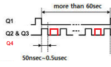
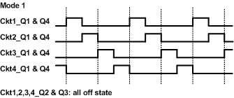
I would like to use the UCC21520 isolated gate driver to operate as shown below.

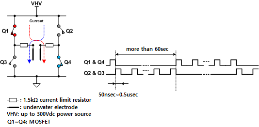
However, I can not control the high-side mos-fet because bootstrap does not work.
Please let me know how I can control this high-side mos-fet with UCC21520 (or a replacement).

Circuit attached with pdf file.

Thank you.

8468.SCHEMATIC1 _ PAGE1.pdf

  • Greetings,

    I am an applications engineer supporting UCC21520. I will help you to answer your question.

    You are encountering a duty cycle limitation, present in all bootstrap supplies. From the timing diagram, one of the low side FETs will always be off for > 60 seconds. VSSA, which is attached to the drain of the low side FETs, will continuously be at a higher potential than VSSB during this interval. Likewise, VDDA will be at a higher potential than VDD during this interval, so the bootstrap supply cannot recharge the VDDA capacitors. Because one channel consumes about 1mA quiescent current, the high-side capacitors rapidly deplete. 

    Because of the extreme duty cycle constraints in this application, I recommend using a separate, discrete isolated supply for each high-side driver.

    Regards,

  • Thank you for your quick reply.

    Under these conditions, I would like an application circuit that can operate as a high-side / low-side switch without using bootstrap power in UCC21520 device.

    Please sketch the application circuit.

    Regards,

    Kwon

  • Hello Kwon,

    Please look at TIDA-01159 for an example of an isolated DC/DC converter powering the UCC21520 driver stage from a single 5V supply. There are two things to note about this reference design:

    1. The winding ratio of the selected transformer (about 2.5:1) is derived based on the control voltage (5V). If a control voltage of 3.3V is required, the windings ratio of the transformer should be adjusted (about 4:1). 
    2. The reference design uses a bootstrap supply for one of the channels. In your application, the low-side drivers could remain powered by VDD, and only the high side drivers would require an isolated supply.

    The linked schematic suggests that there are up to 12 instrument channels, which could result in an impractical number of isolated supplies. In this application, is it possible to activate Q4 during the off time of Q2/Q3, and Q3 during the off time of Q1/Q4? See the edited timing diagram below. This would give the bootstrap supply a chance to recharge and eliminate the need for separate isolated supplies. The timing diagram specifies a maximum on pulse duration of 0.5µs, but no off pulse duration.

    Regards,

  • Hello Derek Payne,

    Thank you for your detailed explanation.
    I now understand that can use isolated power with high-side power.
    I guess I did not have enough explanation about my intentions. I will make it more clear.

    There are four H-bridge circuits as shown below.

    And, there are two operation modes.

    In mode 1, the current flows in the red direction, and in mode 2, the current flows in the blue direction in the order of [ckt1], [ckt2], [ckt3], and [ckt4].

    The switching time between mode 1 and mode 2 can be very long.

    [mode 1 timing]

    [mode 2 timing]

    The on-time of the mos-fet, that is, the pulse width, is about 50 nsec to 500 nsec.

    Please advise me more about this.

    Regards,

    Kwon

  • Hi Kwon,

    If I understand correctly, the following two statements should be true (please verify):

    • When pulse width is about 50ns, there will be approximately 150ns of no activity on each circuit
    • When pulse width is about 500ns, there will be approximately 1.5µs of no activity on each circuit

    If this is true, you should be able to activate Q3 (mode 1) or Q4 (mode 2) for the interval between each circuit's pulse. This will pull VSSA of the active driver to ground, allowing VDDA to recharge through the bootstrap circuit. Since only the low side MOSFET will be on during those intervals, the load (underwater electrode) will not be energized. If it is possible to activate Q3 (mode 1) and Q4 (mode 2) between pulses on each circuit, this would eliminate the need for isolated supplies on VDDA, and the change could be implemented in software (assuming INA and INB are from a controller of some kind).

    One other note: before the sequence of pulses can start, the bootstrap supplies of all circuits must be charged. During startup and while in standby, Q3 and Q4 should both be activated simultaneously to allow the bootstrap supplies to fully charge. This should not affect mode 1 or mode 2 operation.

    Regards,

  • Hello Derek Payne,

    Thank you for your kindly reply.

    I will try using isolated power.
    We will also review the possibility of changing the procedure so that the bootstrap is fully charged.

    I will contact you again if I have more questions later.

    Regards,

    Kwon