This thread has been locked.

If you have a related question, please click the "Ask a related question" button in the top right corner. The newly created question will be automatically linked to this question.

UCC21520: dead time and MOS-FET heat

Part Number: UCC21520

Hi every one,

My circuit is the same half bridge as the circuit in the datasheet as shown below, and the device values ​​are as follows.

Rin=51Ω, Rdt=4.7KΩ, Rboot=Ron=1Ω, Roff=0Ω, Rgs=10KΩ

Cin=33pF, Cvcc=(1.0+0.1)μF, Cdt=2.2nF, Cboot=(1.0+0.22)μF,

Cvdd=(10+0.22+0.1)μF, Chv=(4.7+0.1) μF/450V

MOS-FET=STD1NK60T4(600V, 1.0A, 8.5Ω),

Dboost=MURA160T3G(600V, 1.0A), Doff=Mss1P4(40V, 1.0A)

And Vcc=3.3V, Vdd=12V, Vhv=20~300V


I have two questions.

The first is dead time related questions.

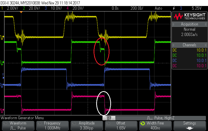
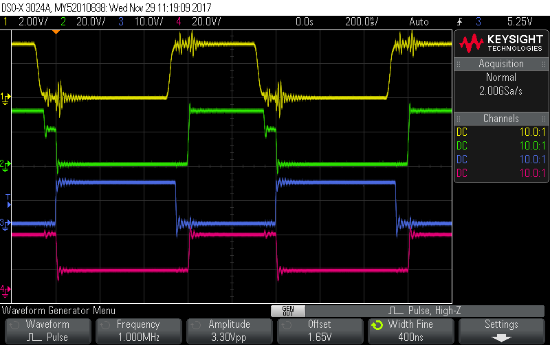
As shown in Figure 1) and Figure 2) below, there is a difference in the dead time waveform between when the high voltage is not applied and when the voltage is applied.(marked red circle).

In what situations does this happen?


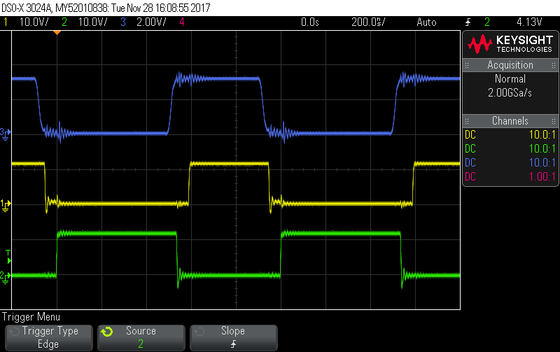
Figure 1) Waveform without high voltage


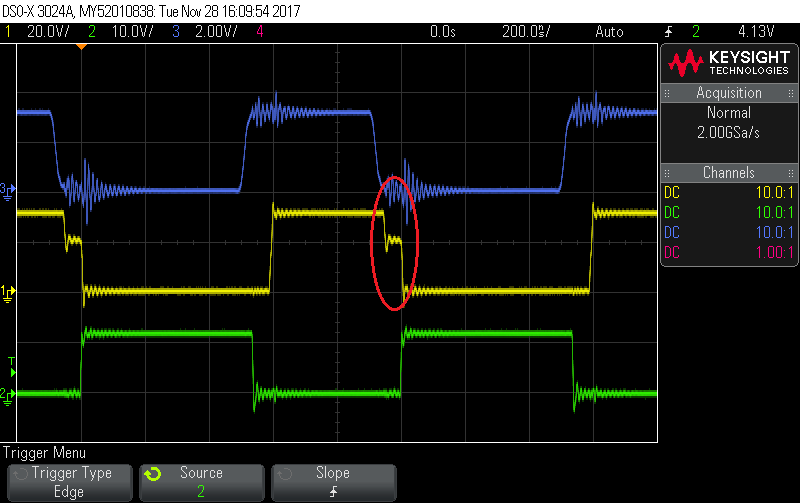
Figure 2) Waveform with 20V high voltage


The second question is about the heat of the MOS-FET.

If a high voltage of 100V is applied, the MOS-FET will generate excessive heat under no-load conditions (ie, when the SW output terminal is open). At this time, the high voltage current is about 13mA.

I want to know the cause of the current flowing and the heat generated the MOS-FET in the no-load state.


Best regards,

Kwon


  • Hi Kwon,

    First Question: please help me confirm about the waveforms:

    • CH1 (yellow): SW
    • CH2 (green): LO
    • CH3 (indigo): HI

    The duration of the event in the red circle is about 50ns, which is roughly the programmed dead time. Even in the low voltage waveform, a small plateau of the same duration can be observed at <1V. I think the dead time circuit is behaving correctly, but it is not possible to tell without a measurement of the HO-HS output. Can this be done using a differential probe or the oscilloscope math function (subtract SW node from HO waveform)?

    The plateau behavior might be explained by a capacitive divider formed at the high impedance node between the high-side and low-side MOSFET. Loading the bridge should help to mitigate this behavior. Let me know if applying a small load (10kΩ) at low voltage (30V) helps.

    Second Question: Is the high voltage current seen when the MOSFETs are switching, or when they are static in off-state? Some current from the high voltage supply should be expected during switching, since the parasitic capacitances of the MOSFETs (Coss) will be charging and discharging. The energy of these capacitors will dissipate in the MOSFETs as heat. But if you see 13mA at 100V with both MOSFETs not switching, then the MOSFETs might not be fully turned off (check Vgs to confirm), the MOSFETs may be damaged (test resistance from Drain-Source, Drain-Gate, and Gate-Source), or the PCB may be damaged (test resistances with MOSFET desoldered).

    Regards, 

  • Hi Derek Payne,

    Thank you for your kindly reply.

    I am sorry that my explanation is not detailed.

    In the waveform diagram of the above question, each signal is shown below.

    In addition, this waveform is the same common in which all power is not isolated.

    • CH1 (yellow): OUTA

    • CH2 (green): OUTB

    • CH3 (indigo): INA (INB=inverted INA)

    What are the HO and HS mentioned in your explanation?

    Figure 3) is a waveform of the same conditions as the above questions.

    Figure 3)

    • CH1 (yellow): INA (INB=inverted INA)

    • CH2 (green): OUTA

    • CH3 (indigo): OUTB

    • CH4 (red): SW(=Vssa=drain pin of low side FET)

    I think that if the flat part of the red circle is dead time, the white circle should be in the low state.

    And the CH4 in Figure 4) is Vdda.

    Figure 4)

    You can see in Figure 4 that the CH4 waveform is rising by Vdd.

    Regards, 

    Kwon

  • Hello Kwon,

    I apologize for the HO/HS terminology. For non-isolated half-bridge drivers (which I also support), the high-side outputs are labeled with HB-HO-HS for VDD-VOUT-VSS, respectively. Similarly, LO is the low-side output. I will make sure to use the appropriate terminology for UCC21520 in the future.

    Thank you for the new waveforms, they are very clearly labeled! Now that I know OUTA is referenced to GND, this waveform makes sense.

    1. After activating the high-side MOSFET, you have charged up to high voltage the drain-source parasitic capacitance on the low-side MOSFET.
    2. When the dead time begins, both outputs go low and both MOSFET drain-source paths become high resistance, so there is no path for current flow for the low-side MOSFET drain-source capacitor.
    3. The parasitic capacitor will hold at high voltage until the dead time ends and the low-side MOSFET activates, creating a path for current flow.

    This can only happen because the half-bridge is not loaded.

    Regards,

  • Hi Derek Payne,

    Thank you for your kind and detailed reply.

    The same waveform is shown in Figure 3) when a 1.5k Ohm load is connected between SW and GND for the discharge path of Cds (drain-source capacitance) of the low-side MOSFET you mentioned.

    In other words, there is no change in the waveform displayed by the red circle and white circle in Figure 3).

    Is it okay to have these waveforms in the half bridge circuit?


    And how do I handle the heat of the MOSFET mentioned in my first post?


    Regards,

    Kwon

  • Hi Kwon,

    It should be okay to have these waveforms in the half-bridge circuit, since the voltage is within the ratings of the MOSFET and the gate driver.

    The total capacitance of the low-side MOSFET Cds from 20V to 10V remains close to constant, and we can conservatively estimate it as about 30pF from the datasheet graph (Figure 11, Coss - Crss = Cds). But if the voltage of the low-side Cds decreases, that means the voltage of the high-side Cds has to increase as well. That capacitor is hard to estimate since it is highly nonlinear in the 0-10V region, but worst case it looks to be around 100pF so we'll conservatively use that number for the whole region. These capacitors will combine in parallel and the time constant for 130pF * 1.5kΩ = 195ns, so conservatively at least (1 - e^(-50ns/195ns)) = 22.6% change would be expected. This is assuming purely resistive load. Since you say there is no change in the white circle in Figure 3, even with a 1.5kΩ load, you should check that your load does not have substantial parasitic capacitance at your operating frequency.

    The switching losses due to Cds will cause the MOSFETs to heat up a lot, and this is unavoidable since the load is too high resistance to dissipate most of that energy. In the waveform, you are switching high voltage MOSFETs at 1MHz, and switching losses are directly proportional to frequency. Reducing the switching frequency, or at least the number of switching transitions per second, will reduce switching losses. You must ensure that your MOSFETs have adequate copper area for heatsinking. They may require active cooling. If you can find another MOSFET with similar ratings and lower Cds, this will directly reduce the switching losses as well.

    Regards,

    Regards,

  • Hi Derek Payne,

    Thank you very much for your thoughtful advice.
    I will solve this problem slowly with time.
    Thanks again.

    Beat regards,

    Kwon