This thread has been locked.

If you have a related question, please click the "Ask a related question" button in the top right corner. The newly created question will be automatically linked to this question.

TPS2549-Q1: C(comp) and R(fa) calculation

Part Number: TPS2549-Q1

Hi,

I'd like to seek your advise on how to calculate the C(comp) and R(FA) values?
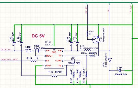
customer of mine is using RT2872 to connect to TPS2549-Q1

Can I assume the following values are fixed in calculation?
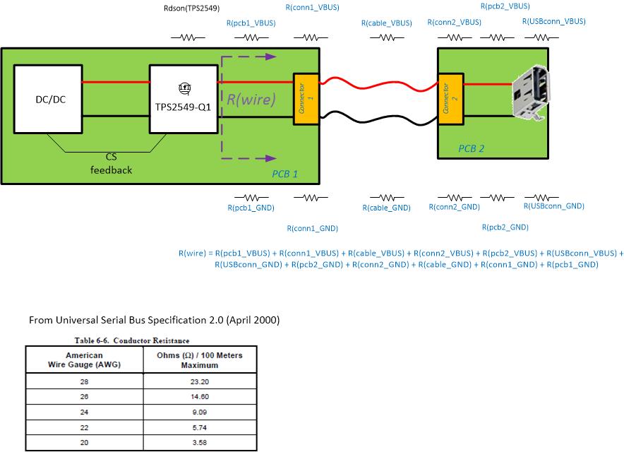
G(cs) = 0.075
R(total) = 0.42ohm

Thanks

  • Hi,

    Please follow below procedure, you can also find it in Page18 of TPS2549-Q1 datasheet.

  • Hi Yongqiang,

    Thank you so much for your advise.
    I do understand the design guideline in datasheet pg18. but what I do not comprehen are the derivation of rds(on), G(cs) and R(wire)

    Can I assume the following values:
    - rds(on) = 0.42ohm? (is this value get from the upper MOSFET of DCDC or the power switch itself)
    - G(cs) = 0.075?
    - R(wire) = 0? (how does TI calculate this value?)

    Sorry for the inconvenient caused
    Hope you can give me some guideline or help to advise the values based on customer's DCDC
    Thanks
  • EL -

    Hope this helps.

    - rds(on) = on-state resistance of the internal FET (TPS2549-Q1). Refer to Electrical Characteristics table, page 5. Assume 72 mohm as this is the maximum value over the temperature range -40 to 85C - a common operating temperature for this device.

    - G(cs) = 75uA/A. Refer to Electrical Characteristics table, page 6. For every 1A of current flowing to your USB load, the CS pin will sink 75uA from your dc/dc feedback network to ground. This is what adjusts the dc/dc output voltage to compensate for load.

    Cable compensation is used to offset the effect of IR drops from the dc/dc + TPS2549-Q1 to the USB receptacle. The purpose of cable compensation is to maintain ~5V across the USB receptacle under normal USB load conditions.

    Please refer to attached picture.

    - R(wire) = R(wire) is the summation of all resistance drops from the OUT pin back to the GND pin of the TPS2549-Q1. This depends upon completely on your application and implementation.

    Connectors:

    If you are using custom or automotive specific connectors between pcb1 and pbc2, you should consult the manufacturers datasheet for the pin resistance of these connectors.

    Cable:

    It is common for automotive implementations to have 1m or more of interconnect and cabling between the USB VBUS power source and the actual connector (for example Type-A). The USB 2.0 specification provides estimated wire resistances based upon AWG. Again, consult your supplier to obtain a more accurate estimation if needed.

    Hypothetical Example.  Please determine R(wire) for your exact components.

    rdson(tps2549-q1) = 72 mohm

    R(pcb1_VBUS) = R(pcb1_GND) = 2 mohm

    R(conn1_VBUS) = R(conn1_GND) = 20 mohm

    R(cable_VBUS) = R(cable_GND) = 1m 24AWG wire = 2 x 9.09 ohm/100 = 90.9 mohm

    R(pcb2_VBUS) = R(pcb2_GND) = 1 mohm

    R(USBconn_VBUS) = R(USBconn_GND) = 20 mohm

    R(wire) = 2 x (2 + 20 + 90.9 + 1 + 20) = 267.8 mohm

    RFA = (rdson + R(wire)) / G(cs) = (72 mohm + 267.8 mohm) / 75 uA/A = 4530 ohm

    John