This thread has been locked.

If you have a related question, please click the "Ask a related question" button in the top right corner. The newly created question will be automatically linked to this question.

TPD1S514: VBUS_Power Rise Time

Part Number: TPD1S514

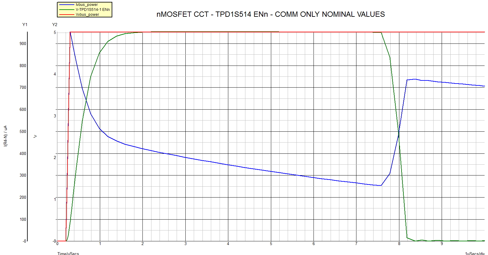
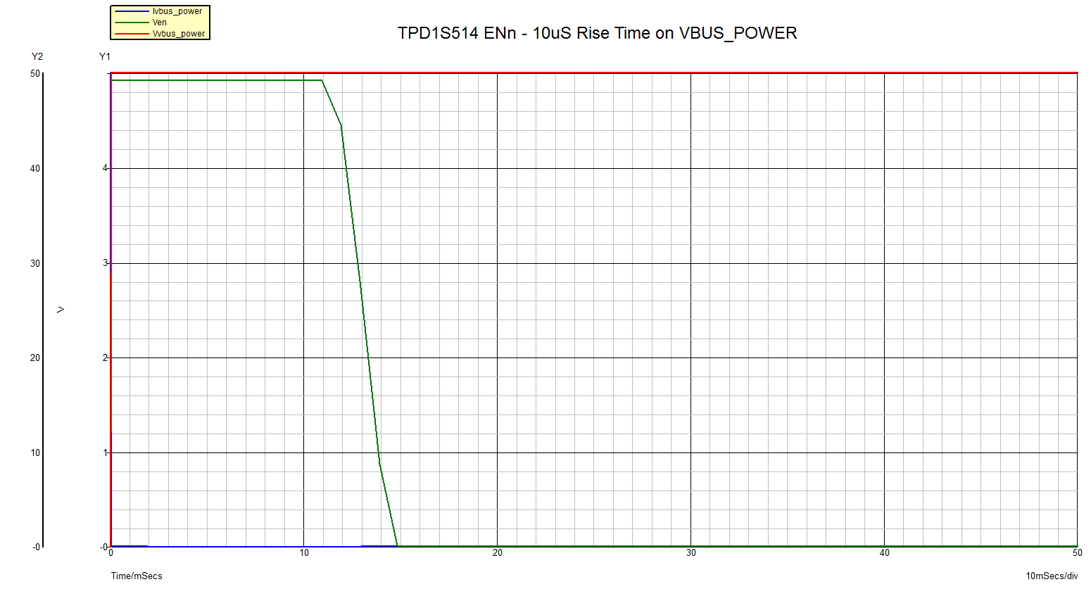
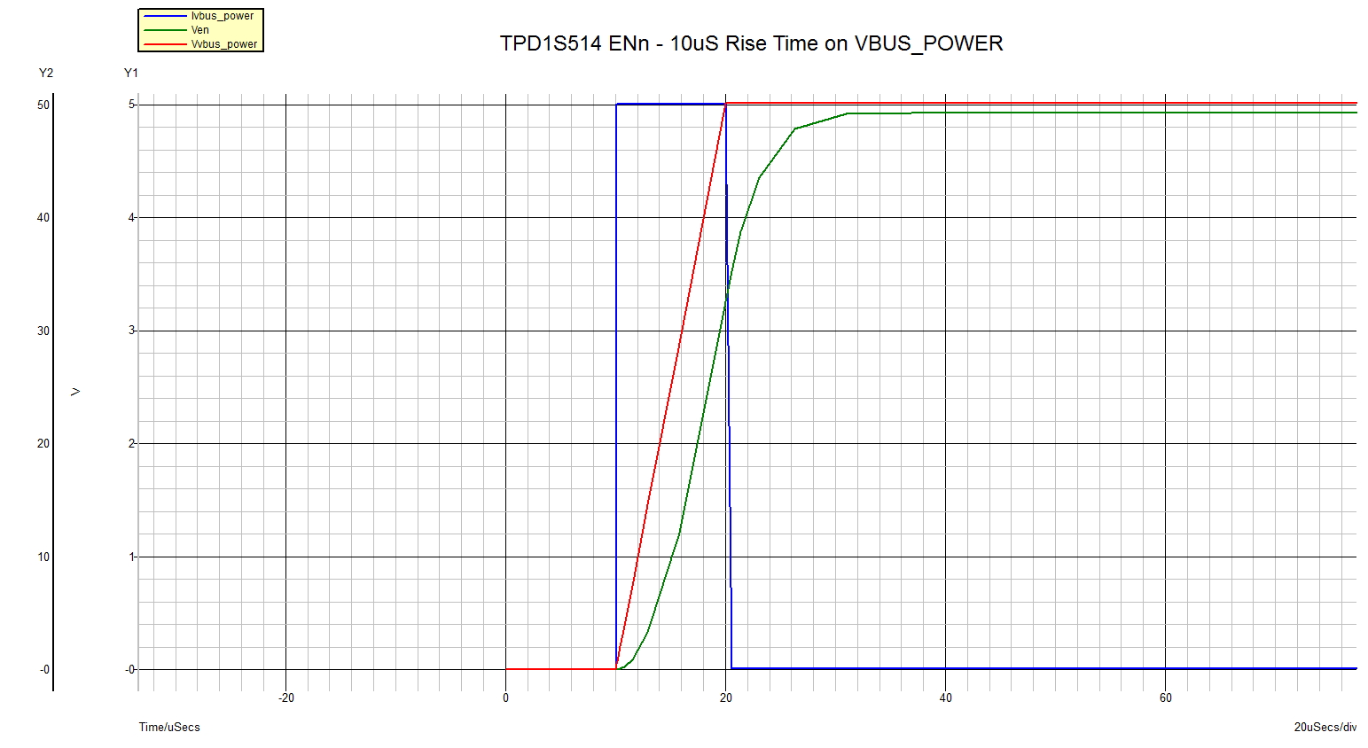
When the TPD1S514-1 is powered by a USB Type C Vbus what is the expected TYP\MAX rise time on the VBUS_POWER ?

  • That is a somewhat difficult questions to answer.

    The allowed capacitance is between 0.1uF and 4.7uF and the max current draw from the pin is 3mA, so the rise time will be determined by the selected value of capacitor and the amount of DC load.

    The circuit is an LDO, so there is no current limit beyond the fact that the LDO will not be in regulation at more than 3mA and this will create a current limit effect, but it is not controlled in the design.
  • Dear Chuck,

    Thanks for your reply

    The reason I am asking is that am using the nmosfet circuit you suggested. I did a SPICE simulation and got good results i.e.

    However then I realised that I might need an additional capacitor on the VBUS_POWER (in accordance with the data sheet as you mentioned -  0.1uF and 4.7uF) -

    1. Is this required in addition to the C1 I have ? 

    2. I realised that my results were very dependant on the rise time of the VBUS_POWER - thus I was wondering what value I should put into the simulator  ?

    Bets regards

    Shmuel 

  • Shmuel,

    The capacitance is required in addition to the C1 in your figure. This capacitor is necessary to stabilize the control loop of the LDO providing the VBUS power.

    I would suggest a value that matches another cap in your system. The exact value of this capacitor doesn't matter as long as it is within range. It appears that the enable pulse has a very good width that should give you good margin even with any change because of the rise time of the

    In your spice simulation, you will not see the impact of adding this additional capacitor unless you change your 0 ohm resistor to a 1-2 ohm resistor to model the pass device. I don't have characterization data on the pass transistor to provide you, but because the LDO is limited to 3mA of output current, I would say that 500 mohm to 1 ohm is a good estimate to use for this simulation.
  • Chuck,

    The 0 Ohm resistor was only a fake so that I could get a good current reading.

    When I added the capacitor on the VBUS_Power the current drawn was very high until I realised that it was dependant on the rise time of the VBUS_Power. If I place a 1uF Cap what scale of rise tiem do you think I will get ?
  • Shmuel,

    With this type of circuit is is a little difficult to estimate because I don't have data on how the regulator will perform. It will charge somewhat like a resistor while the voltage is rising because the LDO will not be in compliance initially, then will start regulating once the capacitor is charged and the current reduces.

    I did take a look at figure 6 in the spec, and if your system uses the recommended capacitor values, it is a good assumption the VBUS_POWER will track the VBUS_CONN rise time very well, so you can use the VBUS_CONN rise times for your simulation.

    Regards,
    Chuck
  • Chuck,

    Where can I get the VBUS_CONN rise times info ?

    Regards

    Shmuel
  • Shmuel,

    Any information that is out there should be in the Type-C specification. I know that the VBUS capacitance is controlled and there are current limits for power providers.

    Between those two values, you should be able to estimate the range of rise times possible.

    Regards,
    Chuck
  • Dear Chuck,

    I looked around and found the max rise time for VBUS is 100mS. I actually went and took my own measurements and found that its rise time was approx 10mS on the specific computer I used. The problem is I have to deal with 2 extreme scenarios :-

    1. A cold start up - VBUS rise approx 10mS - 50mS (when my device is plugged into a computer \ USB power supply that is not powered and then the power is turned on )
    2. When my device is plugged into a usb port that is already powered (VBUS already present at full voltage) - thus the rise time on my VBUS could be 20nS - 50uS

    Best regards

    Shmuel
  • Shmuel,

    I agree with your calculations. The circuit I gave you should be very robust to situation #2 with a fast rise time. The design challenge will will be to size the resistive divider for the gate fet and the capacitor size to meet the 50ms rise time case.

    Regards,
    Chuck
  • Dear Chuck,

    So I now assuming that the min rise time of the VBUS_Power will be 10uS with the recommended 1uS on VBUS_CON and 0.1uS(min) on VBUS_CON. However according to my SPICE simulation this causes a very short spike in current the width of rise time well above the 3mA limit.

    Please advise ?

    Best regards

    Shmuel
  • Shmuel,

    Can you give me the waveforms and the schematic of your spice simulation?

    Regards,
    Chuck
  • Chuck,

    No problems - below is the schematic

    Here is the simulation :-

    and the zoomed in to see the current 

    Best regards

    Shmuel 

  • Shmuel,

    There is no limiting resistance connected to the C2 capacitor, so you will see high currents as that capacitor charges and discharges in your spice simulation. The 100k resistors will prevent the other legs from drawing current, but the 100nF capacitor will have to charge. Most USB circuits have 1uF to 10uF out load cap on the VBUS rail, so this capacitor should be within the expected current draw of the system.

    The 3mA is typically looked at as a steady state current after the device has been plugged in , but before it is enumerated.

    Regards,
    Chuck
  • Dear Chuck,

    Do you think I need to put a resistor in series with C2 to limit this current spike ?

    Regards

    Shmuel
  • Shmuel,

    I do not think that the resistor is necessary. The circuit meets the spirit of the USB specification and should not cause on compliance issues.

    Regards,
    Chuck