This thread has been locked.

If you have a related question, please click the "Ask a related question" button in the top right corner. The newly created question will be automatically linked to this question.

TPS2553-Q1: About internal equivalent circuit of TPS2553-Q1

Part Number: TPS2553-Q1

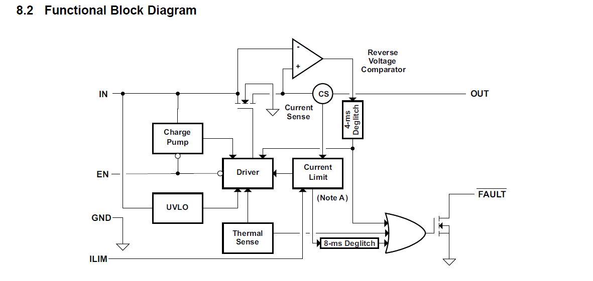
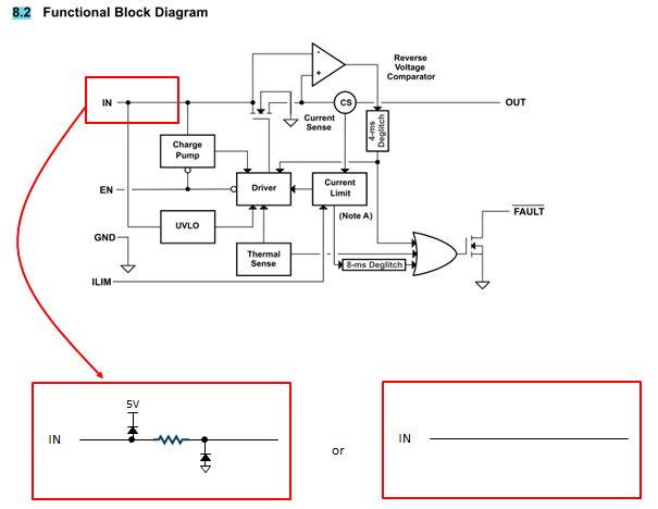
Customers are considering TPS2553-Q1.
The following request was received from the customer.

Q.
Please provide internal equivalent circuit of TPS2553-Q1 all pins.

*
The reason for requiring an internal equivalent circuit is as follows.

1)Check the presence of clamps
2)Checking bias current

Could you provide me with this information?

-Harukawa

  • Hi, Harukawa,

    Does functional block diagram in datasheet satisfy customer's request?

  • Thank you for your reply.

    I understand that Figure 8.2 shows the internal circuit configuration of TPS2553-Q1.
    However, what the customer want to confirm is the presence or absence of a clamp circuit (ESD diode) at each pin (e.g.IN input).

    Q.
    Is it possible to present an internal equivalent circuit as shown below, for example?

    -Harukawa

  • Hi, Harukawa,

    There is a clamp circuit at each pin and it's ESD diode. But the circuit is not like what you attached, sorry that I can't present any equivalent circuit because it's kinda confidential.

    Bob
  • Thank you for your reply.
    The customer understood that the internal equivalent circuit was confidential.
    The customer wants to confirm the following again.


    Q1.
    I understand the EN terminal of TPS2553-Q1 as follows.

    "It is possible to apply a supply voltage to the EN terminal when the voltage is not applied to the IN and OUT terminals."
    Is this understanding correct?


    Q2.
    Each pin contains an ESD clamp circuit (between GND).

    ・GND potential = 0V
    ・The VIN/Vout/Fault terminal other than the EN terminal is 1v or less

    In such a case, does not it occur that the abnormal current flows from the EN terminal to each circuit in the IC?


    Q3.
    Is there a possibility of a sneak current from the EN terminal to the Vin/Vout terminal due to a diode circuit or the like?

    We look forward to hearing back from you.
    -Harukawa

  • Hi, Harukawa,

    Q1: It's correct. You can apply EN before you apply Vin, as long as EN voltage is not beyond recommended operating range.

    For Q2 and Q3, I need to discuss with designer or test it on bench. I will reply you next week.

    Besides, I am curious why customers care current on EN pin so much? If it's just a application that apply EN first then apply Vin, I can guarantee that there's no problem with this case. Because we have validated this kind of start up case before the part was release to market.

    Thanks.

    Regards,
    Bob
  • Hi, Harukawa,

    Sorry for my late reply and not sure why you didn't reply my question. Here's my update for Q2, Q3.
    Q2: It's correct that each pin contains an ESD diode between GND. The diode can be measured by DMM, around 0.54V-0.55V. I measured current when I only apply EN, seems no abnormal current. If there's current, it should be very small, like several uA. If you want to know detailed current, I can ask designer about this for you.
    Q3: I tested, no diode from EN to Vin, and when I apply EN and short Vin/Vout, no current sneak from EN.

    And just like I said before, the application that apply EN before Vin is guaranteed, we have validated it before RTM.

    Thank you.
    Bob
  • Thank you for your answer.

    > Besides, I am curious why customers care current on EN pin so much?

    I asked the customer about this, but there was no answer.
    Sorry for not being able to provide the information.

    > Q2:
    > It's correct that each pin contains an ESD diode between GND.
    > The diode can be measured by DMM, around 0.54V-0.55V.
    > I measured current when I only apply EN, seems no abnormal current.
    > If there's current, it should be very small, like several uA.
    > If you want to know detailed current, I can ask designer about this for you.
    > Q3:
    > I tested, no diode from EN to Vin, and when I apply EN and short Vin/Vout, no current sneak from EN.
    > And just like I said before, the application that apply EN before Vin is guaranteed, we have validated it before RTM.

    I think that customers will be convinced by this answer.
    Thank you for your support.

    -Harukawa