This thread has been locked.

If you have a related question, please click the "Ask a related question" button in the top right corner. The newly created question will be automatically linked to this question.

PCA9306: datasheet 9.2.1 design requirement

Part Number: PCA9306

Hello,

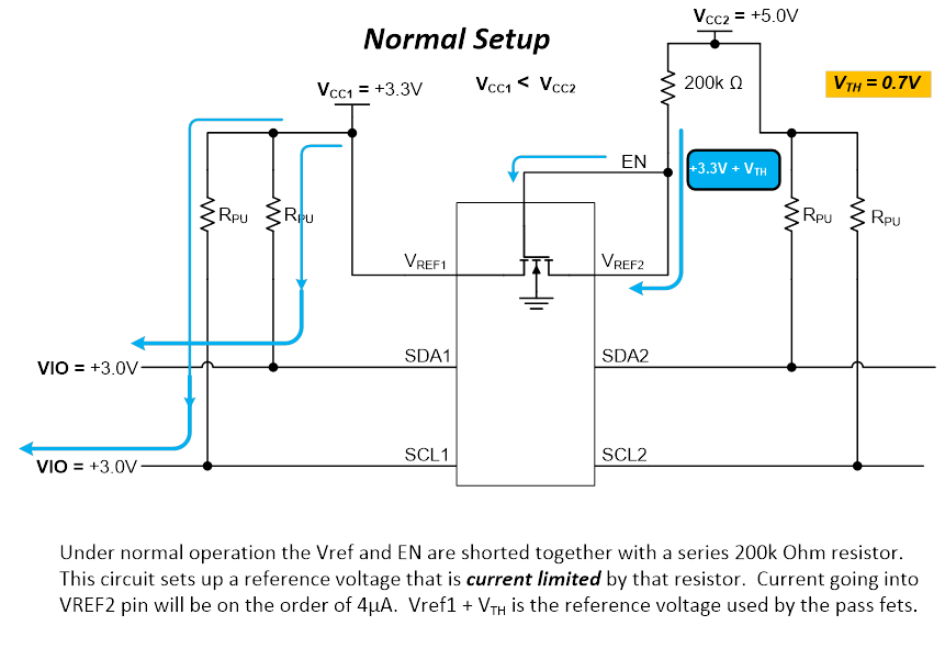
I would like to confirm the meaning of 9.2.1, design requirement in datasheet.

I think this is showing VREF1 + 0.6V <= VREF2 for proper operation. Is my understanding correct?

Figure 7 and 8 are VREF1=1.8V and VREF2 = 3.3V. Is there a reason 9.2.1 typical value is VREF1=1.5V and VREF2=2.1V?

Best regards,

Toshihiro Watanabe

  • Hey Toshihiro-San,

    You can see in the figure below:

    I found Vth in the lab last week to be 0.6V (I only tested one unit though but this makes sense with the minimum requirement).

    You can see with this set up, we are generating a voltage reference onto the EN pin which will be used else where in the device. This reference voltage helps pass lows while minimizing the propagation delays for side 1 and side 2 of the device. If Vref2 is less than Vref1+0.6V then the FET will not conduct and the the reference voltage on EN pin will now be Vref2 which will affect the propagation delays (I found in testing that this prop delays are small), I don't think you will see too much of a difference in the performance of the device by going below the values specified.

    Please realize though, you are no longer following the recommendations set by TI and thus the device may no longer meet datasheet specs.

    With that being said, you will not damage the device by doing this.

    Thanks,

    -Bobby

  • Hello Bobby-san,

    I think your point is Vref1 + Vth < Vref2 is needed for proper operation. Vth is typically 0.6V but it is better to take larger for device varidation. Could I catch your point?

    In 9.2.1, VREF1 typ value is 1.5V.

    In Figure 8, VREF1 is 1.8V.

    I am curious about 9.2.1 ref1 = 1.5V(typ) reason because this value = 1.8V would also seem ok.

    I think this discussion may not be creative so I will stop another post.

    Thank  you for your patience.

    Best regards,

    Toshihiro Watanabe

  • Hey Toshihiro-San,

    "I think your point is Vref1 + Vth < Vref2 is needed for proper operation."
    -Proper operation might be the wrong word here. The device will operate if Vref2 is below Vref1+Vth but it will affect the prop delays most likely. Yes, the device will still isolate the voltages on both side and yes it will still pass a low from one side to the other. The operation of the device will not change but the device may not meet the datasheet specs like the prop delay such that normally the prop delay from side 1 to side 2 with Ven at 2.5V and 30pF max delay was 1.3nS is now 1.31nS. You can see now we promised the device would have a max of 1.3nS but now it has 1.31nS which is not meeting datasheet specs. The device still performs it's job but now it's a little bit slower.

    "In 9.2.1, VREF1 typ value is 1.5V.

    In Figure 8, VREF1 is 1.8V.

    I am curious about 9.2.1 ref1 = 1.5V(typ) reason because this value = 1.8V would also seem ok."

    If the picture had Vref1 at 1.5V, that would still work. 1.8V would still work. Even if Vref1 were at 1.2V, it still works because Vref1+Vth <Vref2 so the device will meet the datasheet specs.

    The device could actually operate if Vref1=Vref2 such as Vref1=1.8V and Vref2=1.8V but in most cases this would be pointless to do because there is no longer voltage translating. What you will see if you do this is, it will take longer to pass a low from one side to the other and will not meet datasheet specs. The device will still operate but will do so slower.

    If you still have any questions or would like to continue this discussion to get more understanding of this device, I am happy to help.

    Thanks,
    -Bobby