This thread has been locked.

If you have a related question, please click the "Ask a related question" button in the top right corner. The newly created question will be automatically linked to this question.

HD3SS3220: USB SS PCB routing

Part Number: HD3SS3220

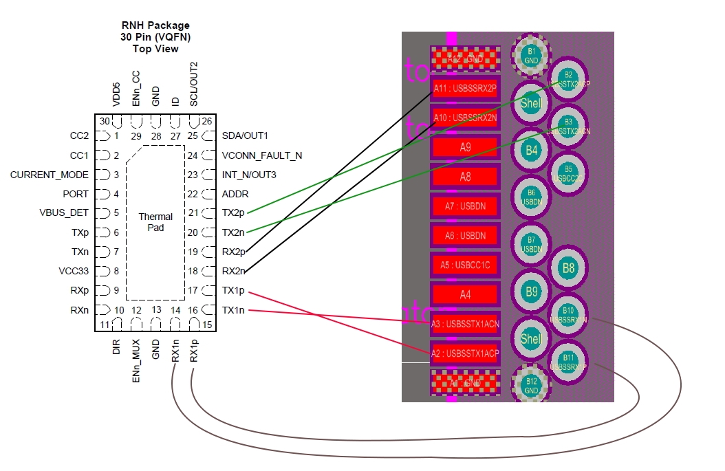
When I placed the HD3SS3220 and my Type C connector (WURTH 632723300011) on the same side of my PCB, most of the signal connections and the routing options seemed reasonable. However there appears to be a cross Tx1P & TX1n shown in red in the diagram below ? (I double checked the pinout of the connector and it is correct)

  • Shmuel

    The lane polarity inversion is automatically handled by the receiver per the USB3.1 spec. So you can route P to N and N to P.

    Thanks

    David

  • Dear David,

    Is this documented in the data sheet for the device somewhere ?

    Best regards

    Shmuel
  • Shumel

    Yes, it is documented in Figurre 11 of the datasheet. The note says "Note: HD3SS3220 Does Not Care About Differential Pair Polarity".

    Thanks
    David
  • Dear David

    Thank you so much for this - this information will certainly help us with our placement and routing !

    I suggest that TI documents this a little better - maybe even put this into a the PCB routing application note with diagrams about routing options.

    The data sheets states "When possible, route high-speed differential pair signals on the top or bottom layer of the PCB" I assume that if and where possible, it would be best to not change layers ? Thus this info that you have provided is going to be critical in the routing of the signals to try and achieve this. Also it would be great if you also put this info in Pin Functions table.

    What about the other side of the chip - the signals that are routed to the FGBA(controller) (TXp/n & RXp/n) can the low and high also be swapped interchangeably ? Since it is not shown on the diagram you outlined for the time being I have not implemented this !?

    Thanks again in advanced

    Shmuel
  • Shmuel

    Routing will depend on the placement of the FPGA and HD3SS3220, the type of USB connector will be used. The idea here is priority should be given to high speed signal routing while minimizing number of via as much as possible.

    On the second question, it will depend on the FPGA supporting lane polarity swap. If it does, then you can swap p and n.

    Once the schematic and layout are finished, I can provide a layout review if needed.

    Thanks

    David

  • Dear David,

    Thank you for your reply. 

    I am using a FTDI FT601 in conjunction with the HD3SS3220

    You mentioned in your first response that "The lane polarity inversion is automatically handled by the receiver per the USB3.1 spec" is something the spec requires or suggests ? Thus is this something that all receivers need to implement or is it optional ? If yes(i.e. required) is my controller, in this case FT601, also considered a receiver and then "required" to implement this functionality ?

    Best regards

    Shmuel 

  • Yes, lane polarity inversion in covered in section 6.4.2 of the USB 3.1 specification. TI cannot confirm if another vendor has implemented this or not, but my interpretation of the specification is that it should be implemented.

    Regards,
    JMMN
  • Thank you