Because of the Thanksgiving holiday in the U.S., TI E2E™ design support forum responses may be delayed from November 25 through December 2. Thank you for your patience.

This thread has been locked.

If you have a related question, please click the "Ask a related question" button in the top right corner. The newly created question will be automatically linked to this question.

UCC21521: Require design help!

Part Number: UCC21521

Hi,

I am trying to design a bidirectional converter using MOSFET IRL2505. Since, my input (Boost mode) can vary from 8V to 16V, I need to select a MOSFET as well as the gate driver to be compatible with a lower Vgs (5V). I found UCC21521 suitable for this application. I will not use Bootstrap technique here, instead, two isolated power supply is used for high side and low side MOSFET. 

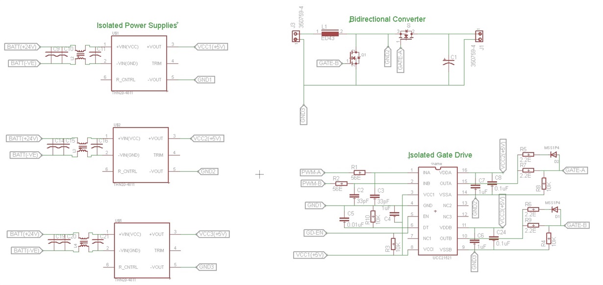
Now, I am little confused while determining gate driver's supporting components. I have chosen all the resistor and capacitor value following datasheet of UCC21521 and I have attached the schematic. Can you please check it once and ensure the design. Thanks in advance.


  • Greetings,

    I am an applications engineer from the high power drivers group. I can help to review this.

    The UVLO turn-on threshold of the UCC21521A is listed in the datasheet as 5.8V typical. The isolated supplies list 5V nominal output, which will keep the driver in undervoltage lockout. I recommend at least 8V supply voltage, to safely cross the UVLO rising threshold and maintain some margin for supply transients.

    This isolated supply is rated for 4A. Was this chosen because of the 4A peak current output of the UCC21521A? When driving capacitive loads, the average current is Qg x Fsw, the gate charge at the drive voltage multiplied by the switching frequency. The peak current is drawn for only an instant, and draws directly from the bypass capacitor. A conservative estimate of the gate charge of the IRL2505 at 8V drive voltage is 200nC (datasheet, fig. 6 + max gate charge at typical conditions), so up to 1MHz the average current per channel will not be much more than 200mA. I think the isolated supplies sourcing VCC2 and VCC3 could be significantly reduced in size without any loss of performance in the application, assuming they only power the gate driver.

    In the application note for the THN 20-4811, the suggested schematic includes a common-mode choke on the input. In the schematic posted, I see several magnetics connected as transformers. As drawn, these transformers would short the 24V supply. Maybe the symbol does not correspond to the actual connection? Please double check this pinout.

    Is the switch node connected to GND2? I do not see it labeled. 

    C17 and C18 are normally used to help meet emissions standards such as EN55022 Class B. They prevent fast common mode transients from developing across the isolation barrier. However, since the output of this isolated supply is presumably referenced to the switch node, these capacitors will constantly be charging and discharging, consuming a lot of power and slowing down the switching edges. I think these capacitors should be omitted, since the switch node is always referenced to GND3 and GND3 is referenced to -VE through C23. If the switch node slew rate needs to be slowed down or emissions standards must be met, consider increasing the value of the gate drive resistors.

    Regards,

  • Hello Mr. Payne, 
    First of all, I want to thank you for your valuable comments on the design. Regarding the placement of common mode chock, that was by mistake. Thank you for pointing it out. The figure is now rectified.

    From your discussion I can understand that for my application,  UCC21521A will not work. Have I understood it properly? Or I can use this gate driver ic with 8V Vgs while the input voltage of my boost converter can goes below 8V. 

    If this gate driver ic is not suitable for this application then can you suggest another one?

    Thank you again for your comments.

    Regards,

  • Hello again,

    UCC21521A will not work with VDDx/VSSx supply at nominal 5V. If 5V isolated supplies are required, a different driver must be used. The minimum UVLO rising threshold on TI isolated gate drivers is >5V.

    The recommended operating conditions in the datasheet for UCC21521A specify a minimum VDDx/VSSx voltage of 6.5V. If you can use an isolated supply which accepts the input range you specify (<8V to 16V) and can produce at least 6.5V output, this is within the recommended operating range of the UCC21521A. I suggested 8V to have margin for supply transients, but it is not a strict requirement. The maximum UVLO turn-off threshold in the datasheet is 6V. This means only 0.5V of margin against supply transients for a 6.5V supply. You must determine what margin against supply transients is required by your application. To summarize: 6.5V is the recommended minimum, but if the application permits increasing the supply voltage above 6.5V, this will improve the margin for supply transients.

    Regards,