Part Number: HD3SS460
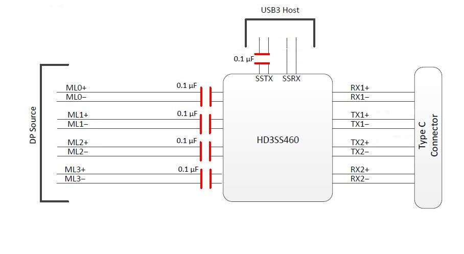
Please refer the Figure3 of HD3SS460's datasheet as below :
The block diagram shows the AC coupling CAP just be implemented on both TX1+/- and TX2+/- near USB TypeC side ,
so please help to confirm how to process the connection of both ML0+/- and ML3+/- between HD3SS460 and DP_source ? (Does it also need any AC coupling CAP?)
And if we've change the design as below , does it have any risk ?