This thread has been locked.

If you have a related question, please click the "Ask a related question" button in the top right corner. The newly created question will be automatically linked to this question.

SN65DP159: dDP159 AUX implementation to FPGA

Part Number: SN65DP159

I am trying to understand the reference design in Application Report SLLA358 (DP159 as DisplayPort Retimer).

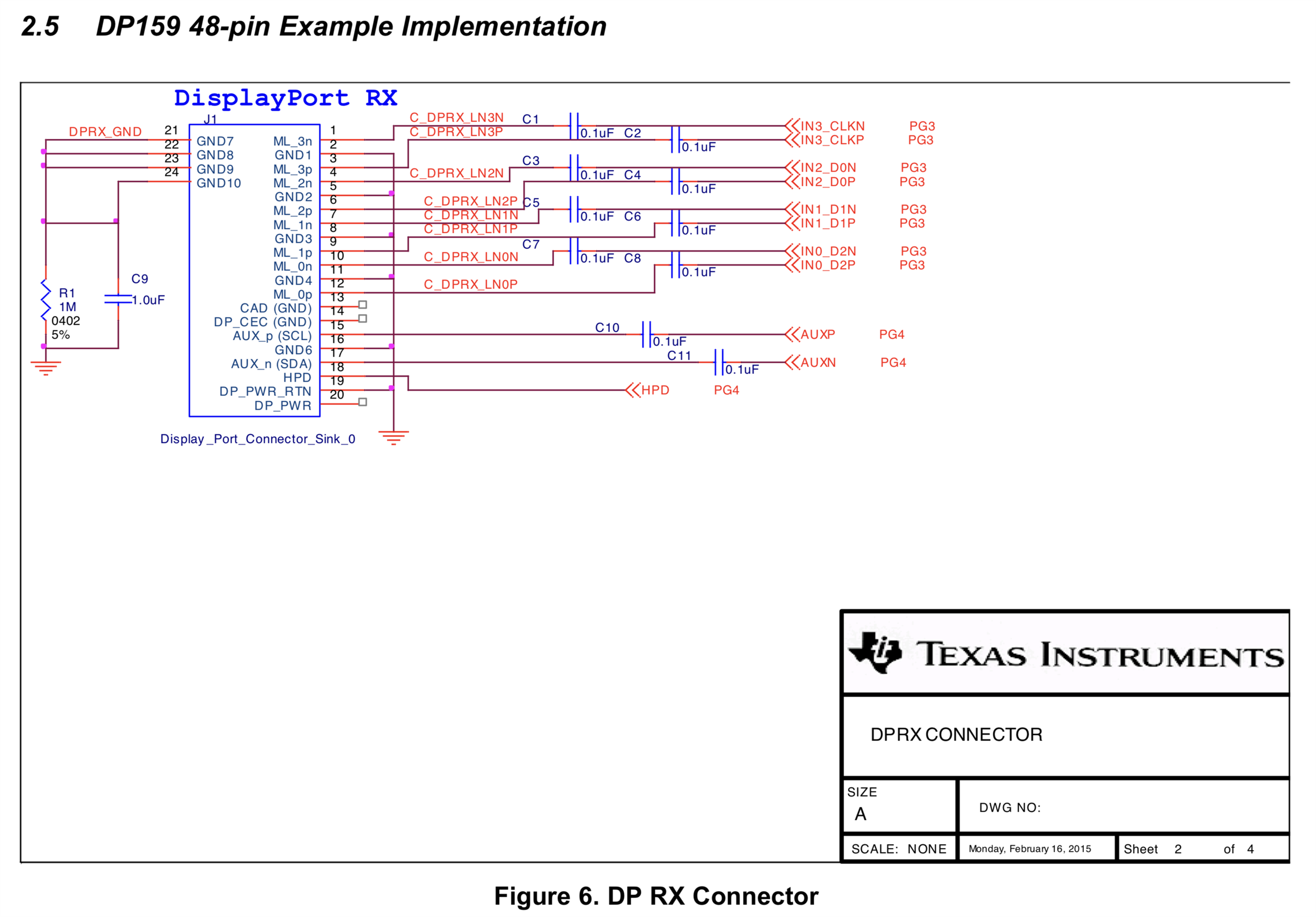
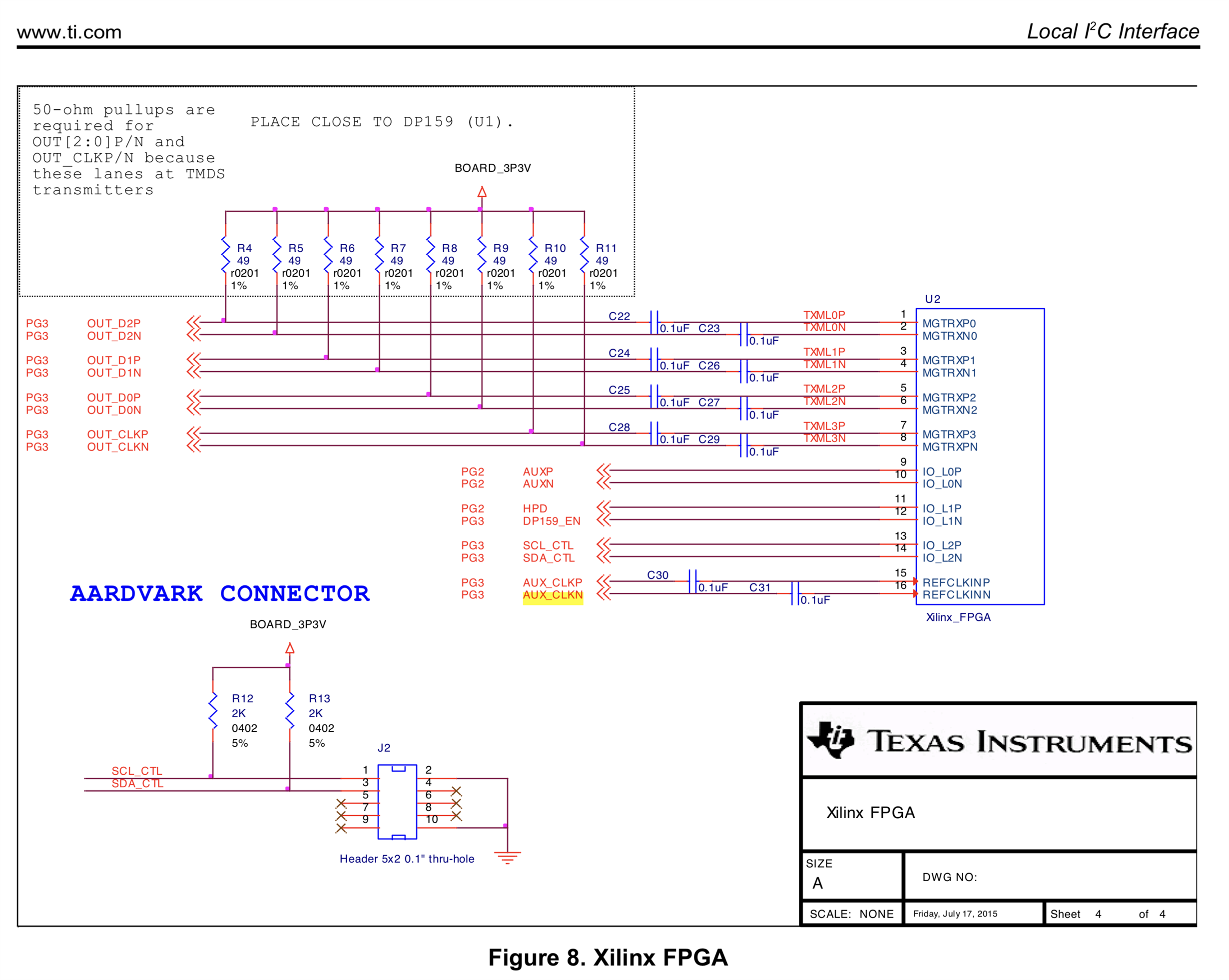
There are schematics on page 5, 6, 7 (attached). In this reference schematic design, AUXP, AUXN (Pin 15, Pin 17 on page 5 of AN) from DisplayPort RX connector are routed to Xilinx (Pin9, Pin10,on page 7 of AN).

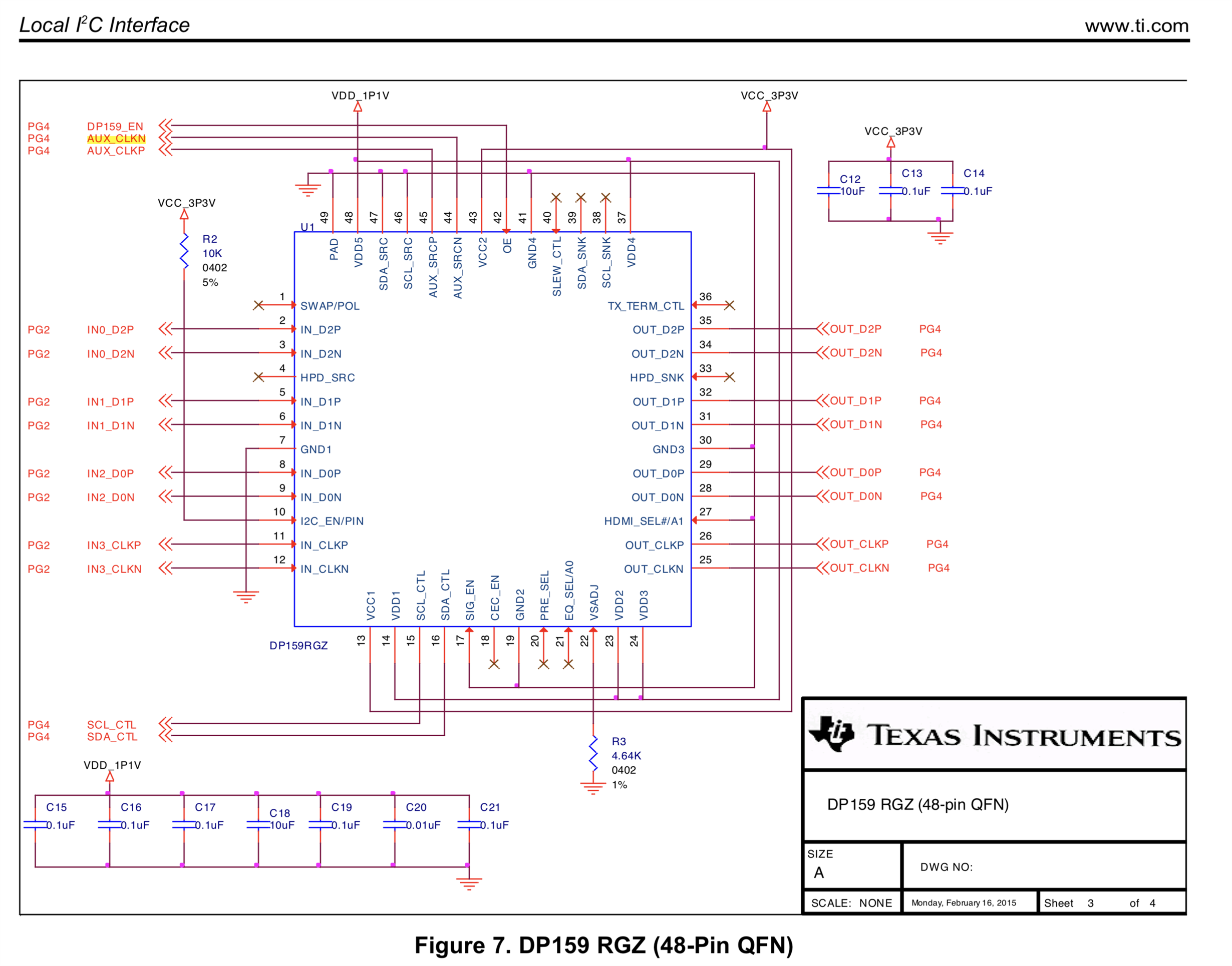
On the other hand, AUX_CLKN, AUX_CLKP (Pin44, Pin45 on page 6 of AN) from DP159 are routed to Xilinx (Pin16, Pin15,on page 7 of AN).

From DP159 dataset Figure 31, AUX (Pin44, Pin45) are used for DP link training between the DP source and DP159.

In this AN, AUX of DP connector is directly routed to Xilinx but not to DP159, how the link training is performed? Is the link training negotiated between DP source and Xilinx? 

In this AN, AUX of DP159 is routed to Xilinx, what is the purpose of this connection?

Thank you.

  • Good Morning Shiwei,

    As stated in section 2.2 in the AN referenced above the DP159 AUX interface can be used to convert I2C-over-Aux to DDC but this is not needed if there is a DP sink. The Xilinx DisplayPort v6.1 acts as the DP sink so the AUX is directly connect and link training is negotiated between DP source and Xilinx directly.In the data sheet the DP159 is instead connect to a HDMI/DVI receptacle therefore the I2C-over-AUX conversion to DDC needs to take place.

    Also, as stated in section 2.2 of AN the DP159 AUX output of a divided clock can help the DP RX to track jitter. 

    I apologize for the earlier post that was sent by mistake.