Other Parts Discussed in Thread: SN65HVD62
Hi, Team
My telecom customer plan to use SN65HVD63 in their smart antenna products.
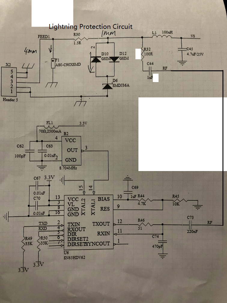
1. They need to add lightning protection circuit on TXOUT/RXIN trace of SN65HVD63. There are several compoenent on the circuit and the PCB trace width is much wider 4mm and 1mm. That will break the 50ohm trace characteristic impedance.
Is there any suggsetion on design the lightning protection circuit?
Here is customer scehmatic:
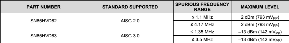
2. In AN65HVD63 datasheet, there is comparison table with SN65HVD62.
Is that all the difference between PHY of AISG2.0 and 3.0?
Is the MAXIMUM LEVEL in the table means the spurious level after the filter integrated in SN65HVD63?

Thanks
Kevin