This thread has been locked.

If you have a related question, please click the "Ask a related question" button in the top right corner. The newly created question will be automatically linked to this question.

ISO5851: ISO5851 DESAT malfunction

Part Number: ISO5851

Hello,

I am currently testing the ISO5851-Q1 as a gate driver for a MOSFET SiC 1200V, on à 650V line.

The 5851 is powered with 3.3V/0V on primary side, and +15V/0V on secondary side (unipolar).

I uses the DESAT function with a 1000V diode plus a 6.8V zener diode, in order to rise the threshold of the desat triggering.

In nominal case, (opening/Closing of the MOSFET, on the 650V/1A line), there is no problem. But when I apply a short circuit on my resistance, leading to a rise of the current flowing, or when I close my MOSFET on a 6501V line wihtout resistance, he DESAT is malfunctionning, leading to the (pretty messy) destruction of the MOSFET.

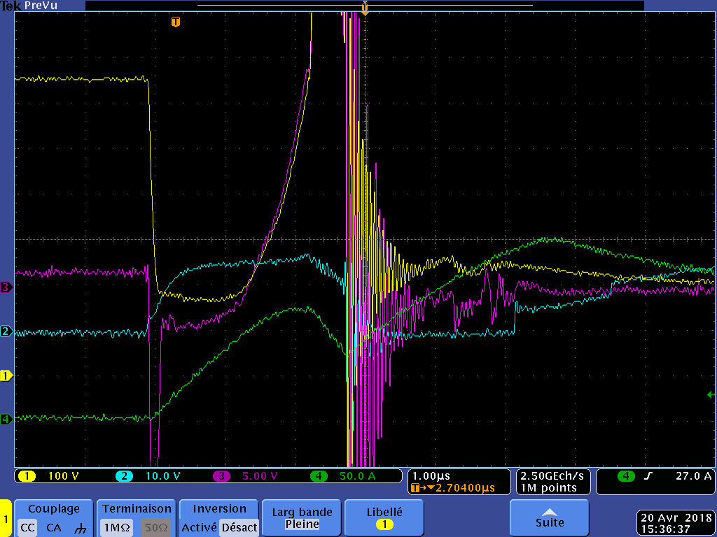
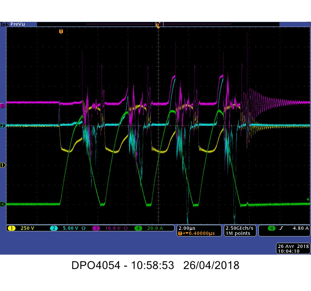
Here is the curves at the fault moment:

- in yellow (acq 1) is the Vds of the MOSFET (650V before the closing)

- in blue (acq 2) is the gate voltage

- in purple is the DESAT voltage

- in green is the current flowing on the 650V line.

we can see the DESAT voltage start to work, but then oscillating and re-closing the gate, leading to the desctruction.

Do you have a clue of the problem ?

Thank you in advance,

Morgan NEDELEC

  • Hi Morgan,

    Thanks for reaching out. 

    1. Could you please share the schematic of the circuits you are testing? Your description is clear but the schematic would give us a more comprehensive picture. 

    2. What kind of probes did you use to measure the signals of VDS, VGS, VDESAT, and ID?

    3. Do you also have the scope capture of the PWM input signal?

    4. What is the condition of ISO5851 after the test?

    With Regards,

    Xiong

  • Hi Xiong,

    here is the schematic of the circuits; note a few changes : D48 is a 6.8V zener diode and D54 is not mounted (0R instead).

    The MOSFET schematic is this, with Q3 not mounted

    To mesure all the signal, we use high voltage differential probes (THDP0200 from tektronix), and current probe TCP0030.

    We don't use PWM but discrete  input (0V/3.3V) from a µC.

    The conditions of the fate driver depend of the destruction of the MOSFET: if the MOFSET explode, leaving an open circuit between collector and Emitter, the ISO5851 is OK, but if it's a SC, the ISO5851 is destroyed as well (SC on VDD/GND primary side).

    Thank you for your concern,

    Morgan

  • Hi Morgan,

    Thanks for the additional info.

    One more question, for the case shown in the waveform, are the driver IC and SIC FET damaged?

    The SIC FET was turned off then turned on after DESAT protection. The false turn on can be due to the Miller effects with high dv/dt, or it is because of the IN+ signal was interrupted.

    Another point, the ID current continues ramp up even when the VGS is low. This may due to the SIC FET is damaged with hard short. Can you please confirm?

    It may also be a good idea to remove the resistor between /RST and IN+ to better locate the root cause. Instead, we can add a pull-up resistor on /RST pin.

    With Regards,
    Xiong
  • Hi Xiong,

    for this case the driver IC is fine, but the SiC MOS is widely open, litteraly :) :

    The Miller effect shouldn't be overrun by the miller Clamp of the gate IC ?

    The IN+ signal has been activated with a cable on a 3.3V extern power supply, maybe it could have a rebound on the plugging?

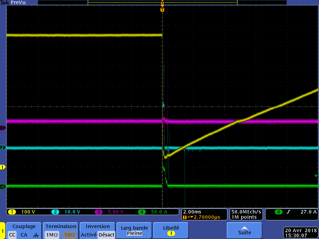
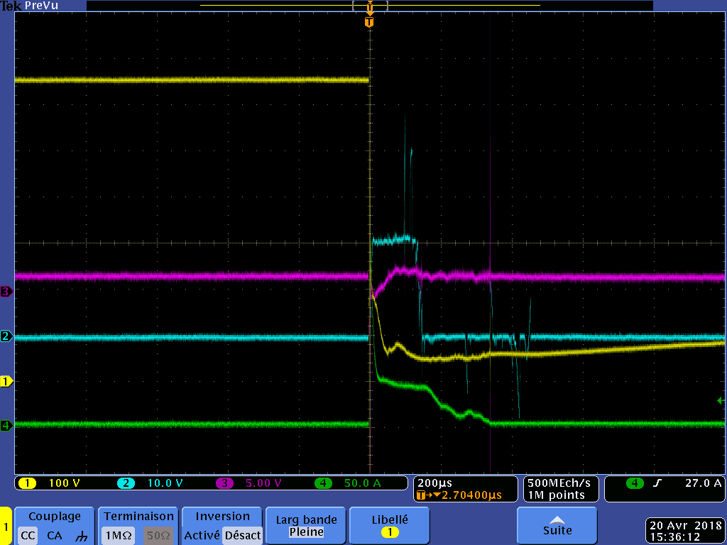
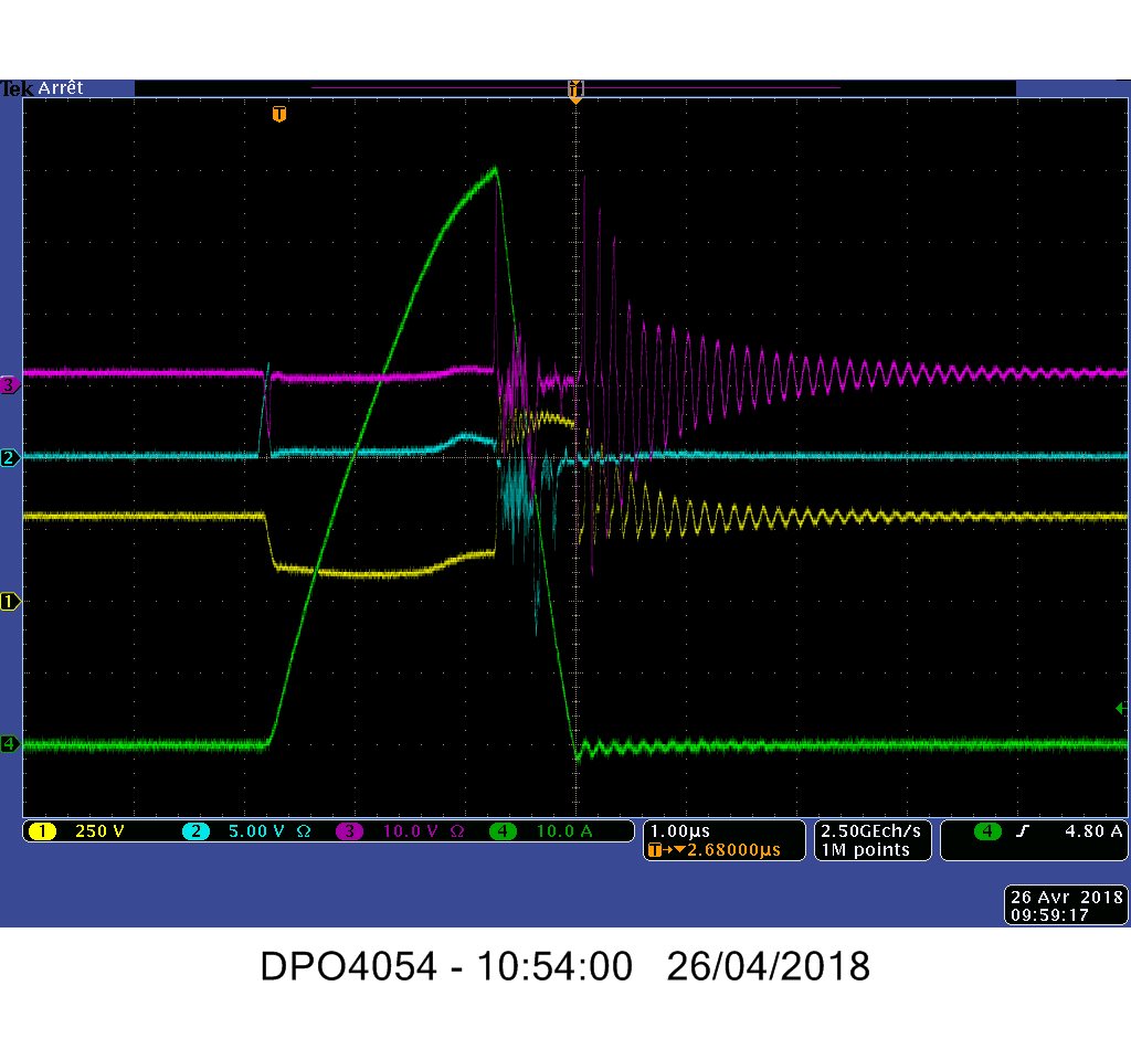
    here is some views with longer time of the same capture:

    what kind of test should I run to locate the root source for you ?

    Thank a lot,

    Morgan

  • Hi Morgan,

    Thanks for sharing the additional info. The new figures you have shared seem to have captured different instants as I could not see the rinings in VDS and ID.

    The Miller clamp function can help to some degree. However, the impedance of the Miller clamp FET is 4Ohm. The gate voltage can't be clamped to low enough to be below the threshold for SIC when the dv/dt induced current is too high. Also, the connection between the gate of the SIC FET to the CLAMP pin of driver IC needs to be short as possible. Otherwise, the effectiveness of the Miller clamp function can be further reduced.

    A few things we can try to help locate the root cause:

    1. Try to replace the resistor with an inductor with moderate value to limit the di/dt rate.

    2. Try to use bipolar power supplies to have better gate clamping when the FET is OFF.

    3. Try to measure the voltage on the IN+ trace to check potential voltage spike and ringing. In the measurement, try to minimize the loop of the probe tips to minimize noise pick up.  

    With Regards,

    Xiong

  • Hi Xiong,

    I've made few more tests to locate the problem;

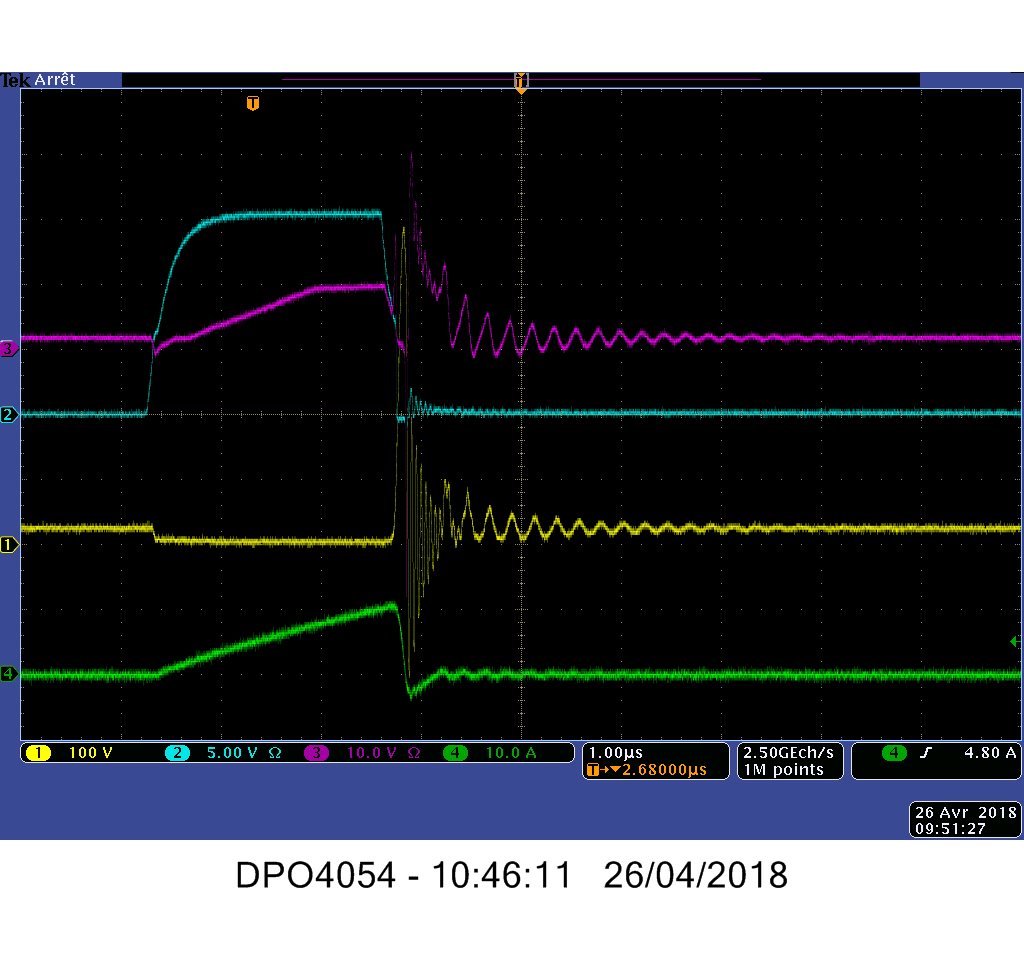
    i've gradually risen the VCE tension to observe the behaviour: we can see that the system is functional, and the DESAT function behave as expected.

    Here is the traces on a 30V CC:

    Here is the traces on a 300V CC:

    But we can can see that it takes 2 µs to the DESAT voltage to activate the DESAT function, and we observe that the DESAT voltage doe not rise the same way on the 300V CC, why this difference?

    Can we adjust this 2µs rise time of the DESAT voltage? I think the main problem in my case is that the di/dt is too high, leading to too much energy to open the MOSFET at 650V.

    I made the test until 500V, where we case see that the MOSFET take multiple attempts to close until success.

    Thank you in advance,

    Morgan

  • Hi again,

    I forgot the 300V CC curves :

    Best regards,

    Morgan

  • Hi Morgan,

    Thanks for sharing the results. Let's talk over phones for more efficient discussions. I have sent you a private message. Please share with me your contact info. Thanks.

    With Regards,
    Xiong
  • Hi Xiong,
    I do not see your PM in my account, could you resend it ?
    Thanks,

    Morgan
  • Hi Morgan,

    Have resent the PM.

    With Regards,
    Xiong