Other Parts Discussed in Thread: TDP158
Hello,
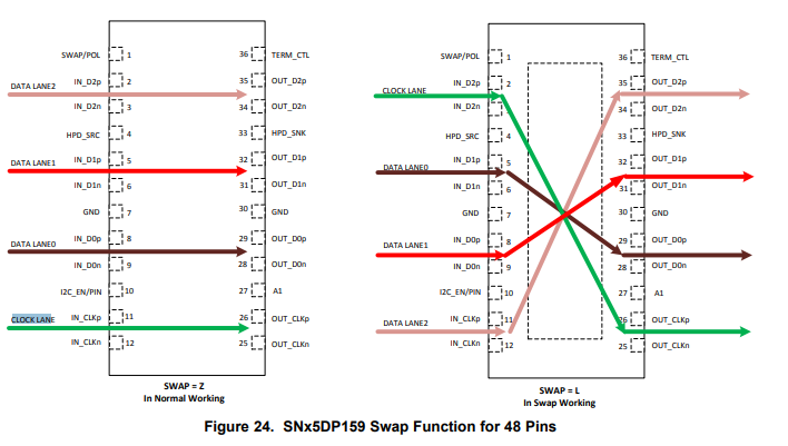
Reading specs of DP159:
In section 7.6 diff inputs characteristics says that max clock lane rate = 340 MHz
In Figure 24: with SWAP = L it shows that data_lane2 is applied to IN_CLK pins
These 2 info are kind of contradicting. I would like to use the DP159 with data_lane2 to IN_CLK, data_lane1 to IN_D0, data_lane0 to IN_D1 and clock_lane to IN_D2 but in normal working SWAP =Z (straight throught). Is it possible when my data_lanex rate is ~ 5Gb/s?
Thanks
Lam Huynh